

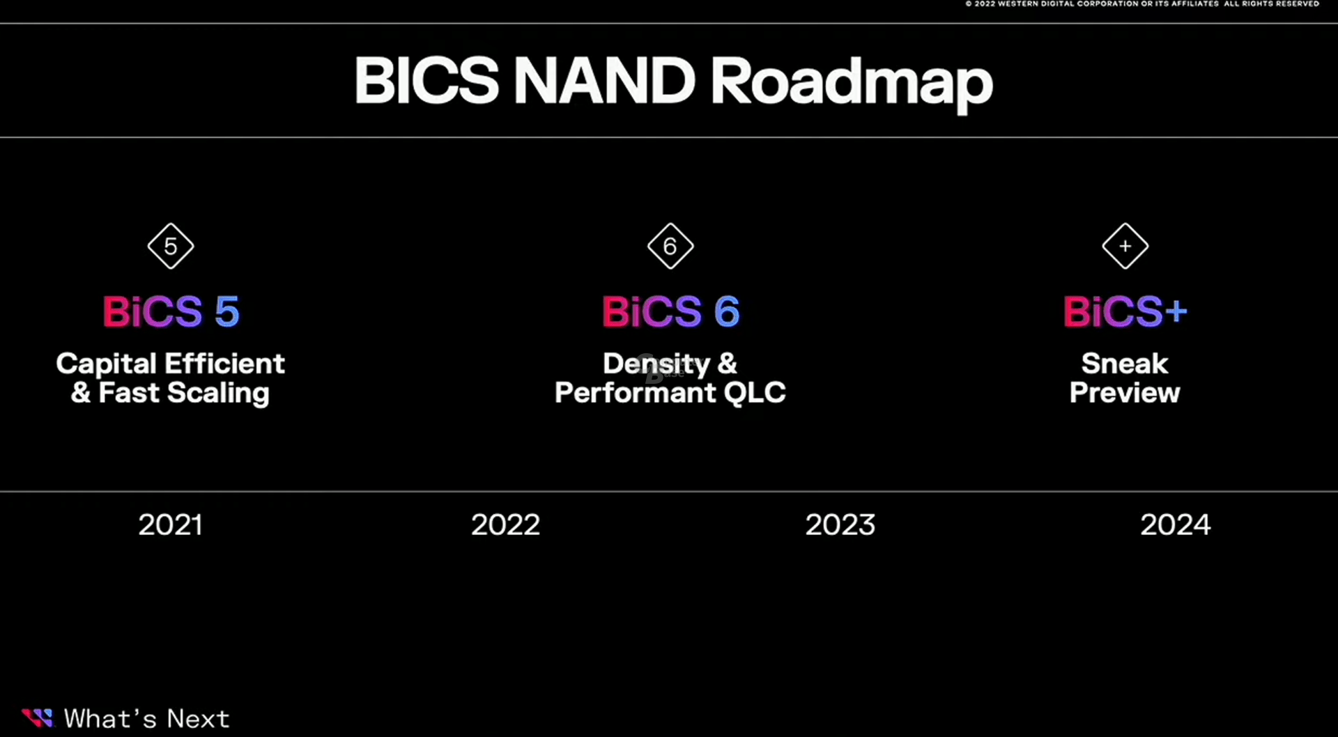
Kioxia and Western Digital are jointly developing the 3D NAND called BiCS Flash. At the Investor Day, Western Digital talked about both the upcoming BiCS6 and its successor “BiCS+”, which is said to represent a “quantum leap in the performance of NAND”.
Currently, the fifth generation (BiCS5) with 112 cell layers is mostly being produced in the factories of Kioxia and Western Digital, which can also be found in more and more SSDs from the two manufacturers. Production of the successor, BiCS6, is scheduled to begin at the end of the year and ramped up in 2023.
BiCS6 as the smallest and fastest QLC variant?
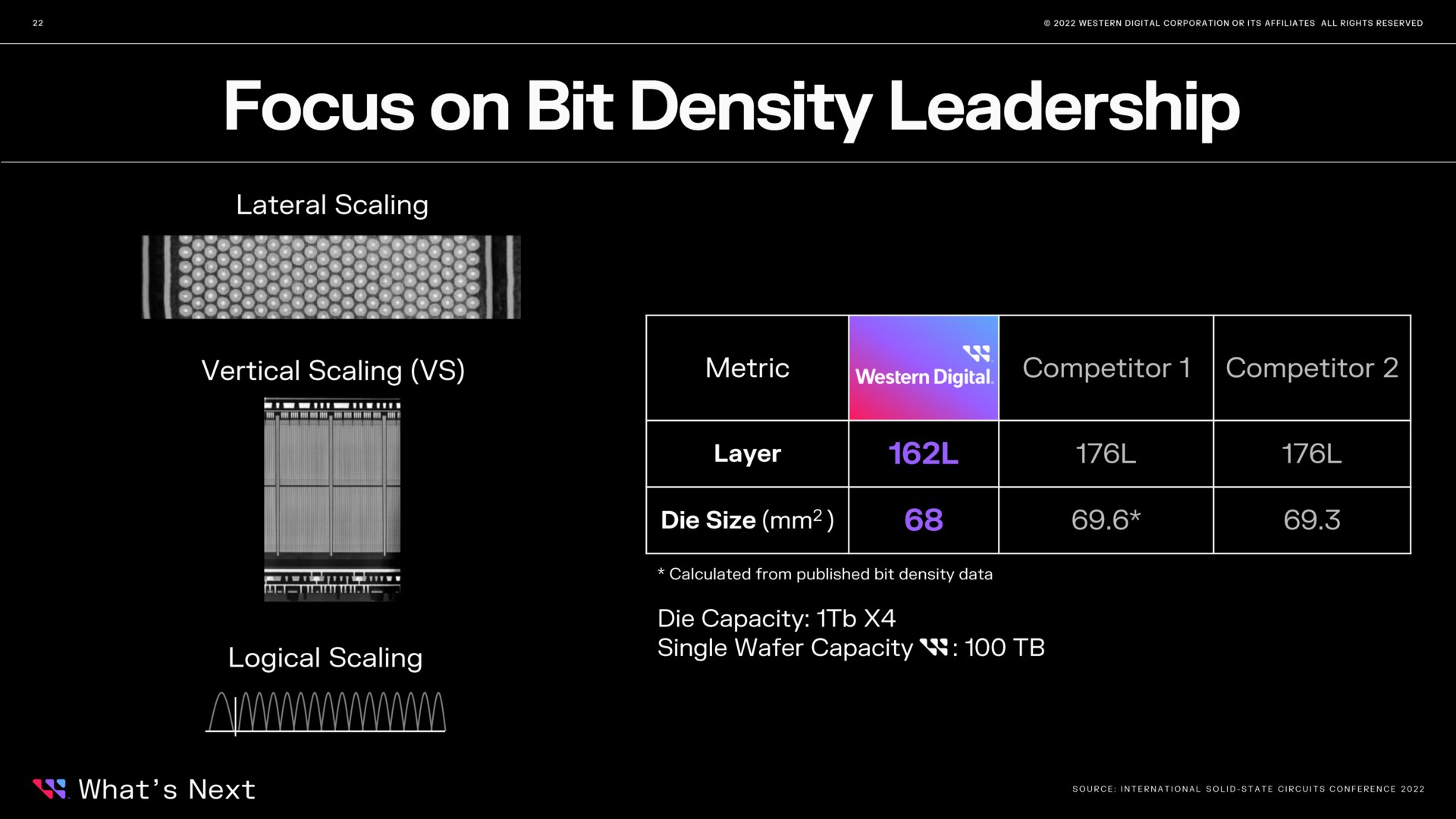
BiCS6 (title picture as scheme) has 162 word line layers and thus fewer than the competitors Micron, Samsung and SK Hynix, who rely on 176 layers. However, the number of levels is not the only important factor, because many other factors such as the size of the cells and their spacing determine the properties of the NAND flash.
Siva Sivaram, President of Technology & Strategy of Western Digital, emphasized in its presentation at Western Digital 2022 Investor Day. More layers by no means automatically mean a higher areal density in gigabits per square millimeter. At least the QLC variant of the BiCS6 is said to be the smallest QLC die with 1 terabit storage volume in the industry at 68 mm². Converted, this would be around 15.1 Gb/mm² and thus more than Intel's 144-layer QLC (13.8 Gb/mm²) or the new 176-layer QLC from SK Hynix (14.8 Gb/mm²). A table compares Western Digital to another 176-layer QLC competitor believed to be Micron.
-
 BiCS6 with the smallest QLC die (and the highest areal density) (Image: Western Digital)
Image 1 of 2
 BiCS6 with the smallest QLC die (and the highest areal density)
  BiCS6 as concept drawing
 Previously, Western Digital and Kioxia had only ever spoken of the faster but significantly larger TLC variant of BiCS6. The new but brief roadmap mentions “density and high-performance QLC”. The great weakness of QLC-NAND, the slow writing, should at least be reduced. The charge-trap cells of the QLC-BiCS6 should be writeable (program) with 60 MB/s. That's more than six times more than BiCS4 (BiCS5 is not available as a QLC) and still 50 percent more than Intel's 144-layer QLC.
-
 BiCS NAND Roadmap
Image 1 of 3
 BiCS NAND Roadmap
 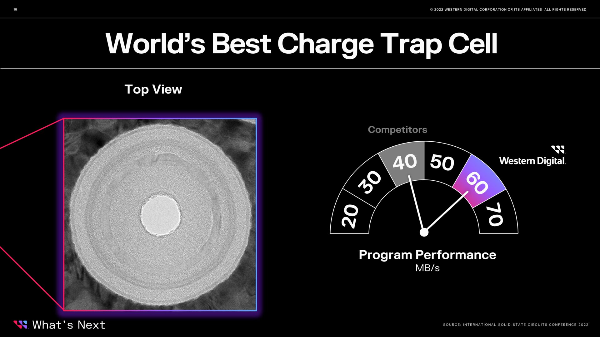 The best storage cell in the world? (BiCS6 QLC)
 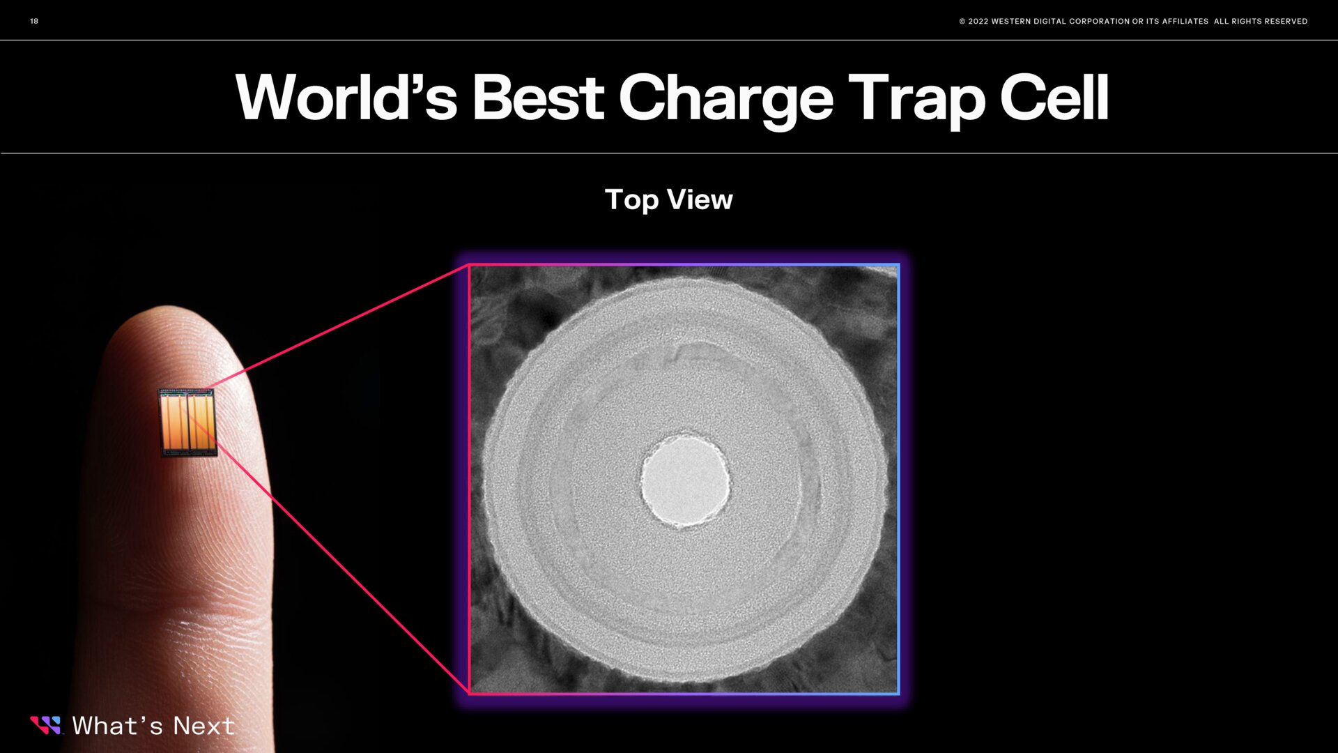 The best memory cell in the world? (BiCS6 QLC)
 BiCS+ with a great performance leap
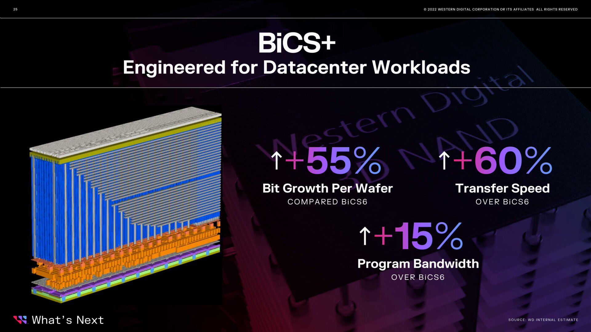
The partners want to keep the cycle of around 1.5 years between the generations and so the next generation is to be presented at the end of 2023. Instead of BiCS7, Western Digital speaks of “BiCS+”. As with Samsung's V-NAND V8, the number of layers should increase to over 200. Due to the once again increased areal density, 55 percent more bits per wafer are promised.
-
 BiCS+ promises significantly more performance (Image: Western Digital)
Image 1 of 3
 BiCS+ promises significantly more performance
 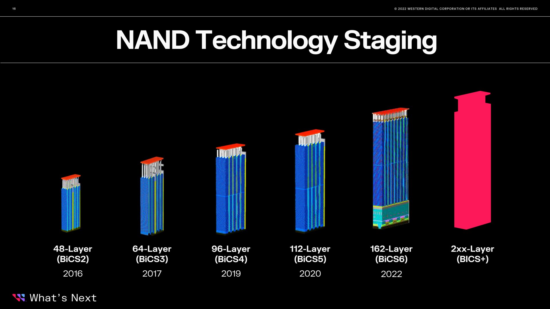 NAND -Generations at Western Digital and Kioxia
 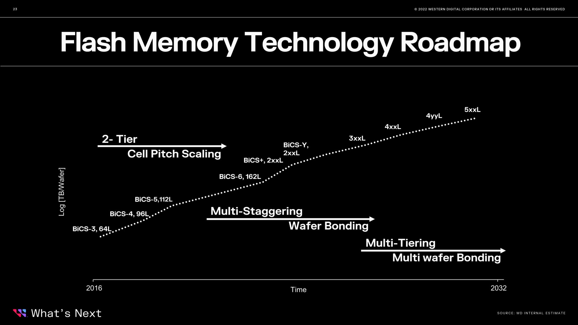 Western Digital: Roadmap for NAND flash technology
 The increase in transfer rates is said to be even greater: no less than 60 percent plus is mentioned here. After all, the programming of the cells should be 15 percent faster.
Sivaram was euphoric and spoke of a “quantum leap in the performance of NAND”. However, further details and corresponding ideas from the competition remain to be seen.
The long-standing partnership with Kioxia in the three joint ventures, the various ways to further increase the areal density of NAND and the lower expenditure for increasing the bit density compared to the competition were also topics of the presentation.
-
 Ways to increase bit density with NAND (Image: Western Digital)
Image 1 of 4
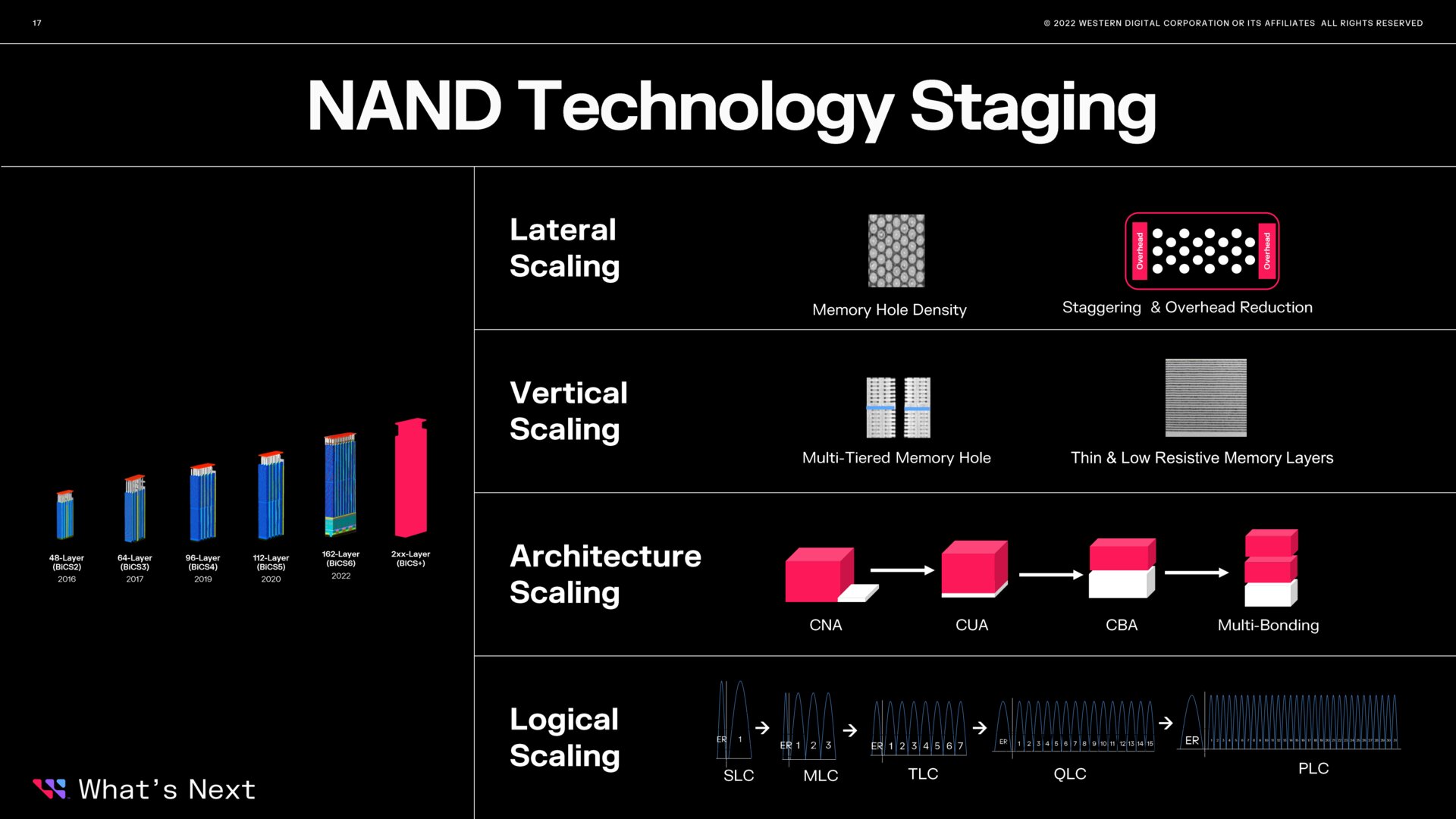 Ways to increase bit density in NAND
 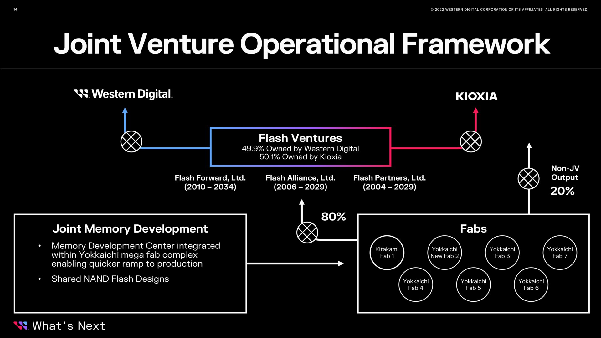 The Western Digital and Kioxia Flash Joint Ventures
 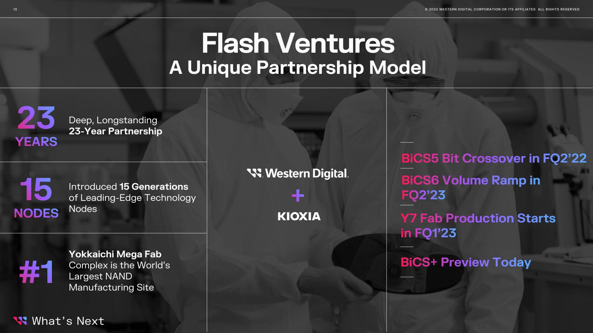 The Western Digital and Kioxia Flash Joint Ventures
 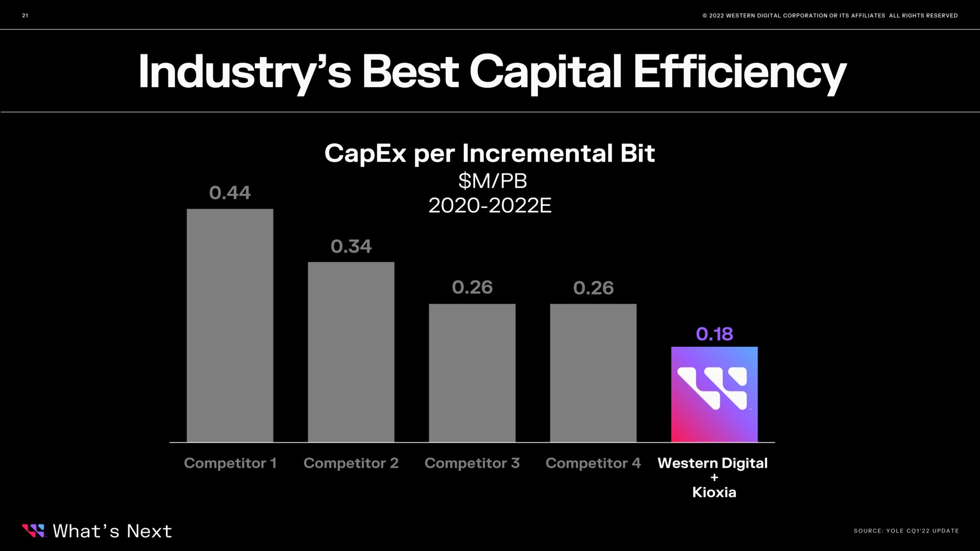 WD and Kioxia spend the least on Bit Growth
 With a total of seven plants, six of which are located in Yokkaichi (Japan), Western Digital and Kioxia together produce more than 500,000 wafers with NAND chips per month. This makes their share of global production around 30 percent.