

Samsung's EUV production has matured so far that five layers are exposed with this technology for the new DDR5 RAM. The chips are based on 14 nm production, or as it is called on the roadmaps in the DRAM industry: 1a.
1a is the current logical step in the Sequence of DRAM manufacturing stages. The last few years were characterized by DRAM chips in 1x, 1y and 1z, now comes 1a, which is also called 1α (1-alpha) here and there. 1a is followed by 1b and 1c, before the first efforts for the next levels 0a, 0b and 0c are made from the middle of this decade. ASML recently presented a suitable roadmap for this, which will extend into the year 2030.
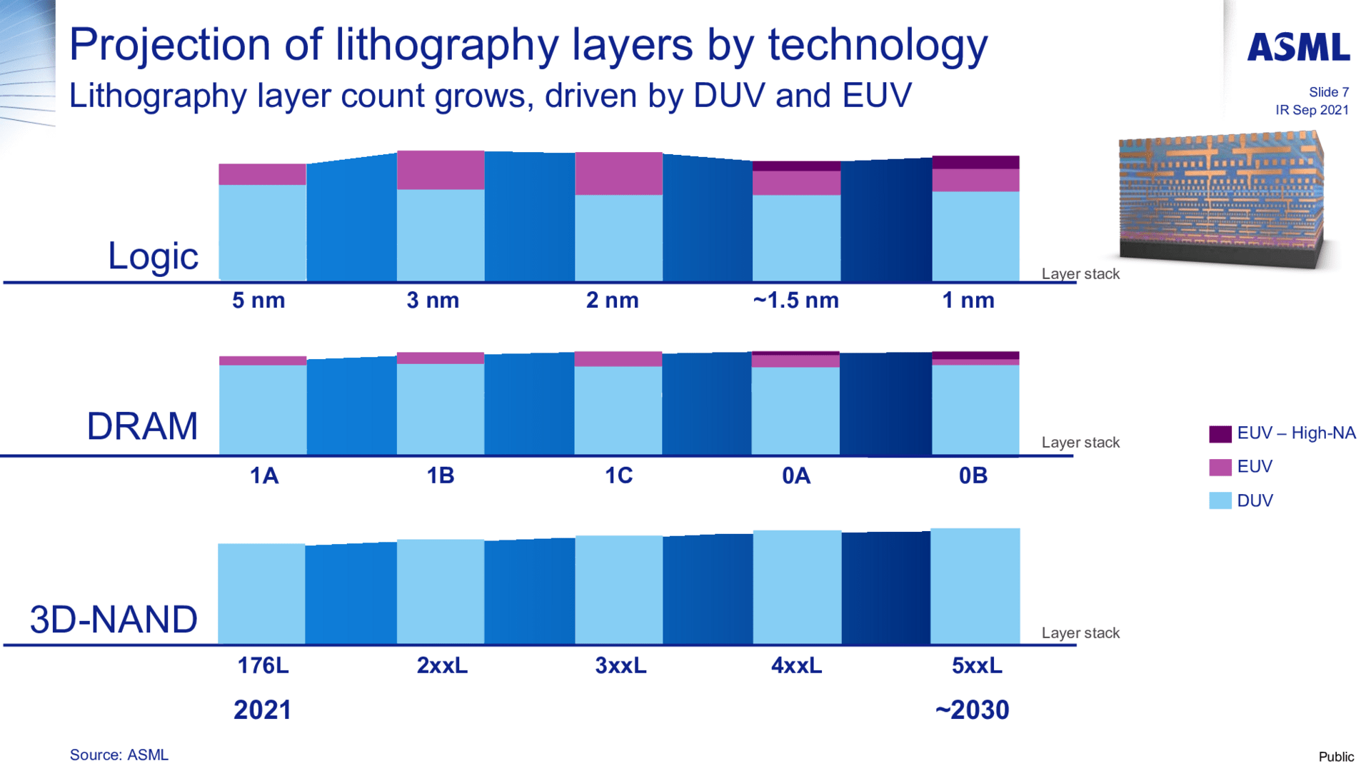
Direct comparisons with the Logic Nanometer Roadmap have always been difficult, since, like CPUs, there are no real nanometer data in it either, but marketing terms are used: the smaller the better. For the first time, however, Samsung dares to switch to a specification in nanometers in its press release: 1a now corresponds to 14 nm in the DRAM language, largely manufactured with EUV exposure.
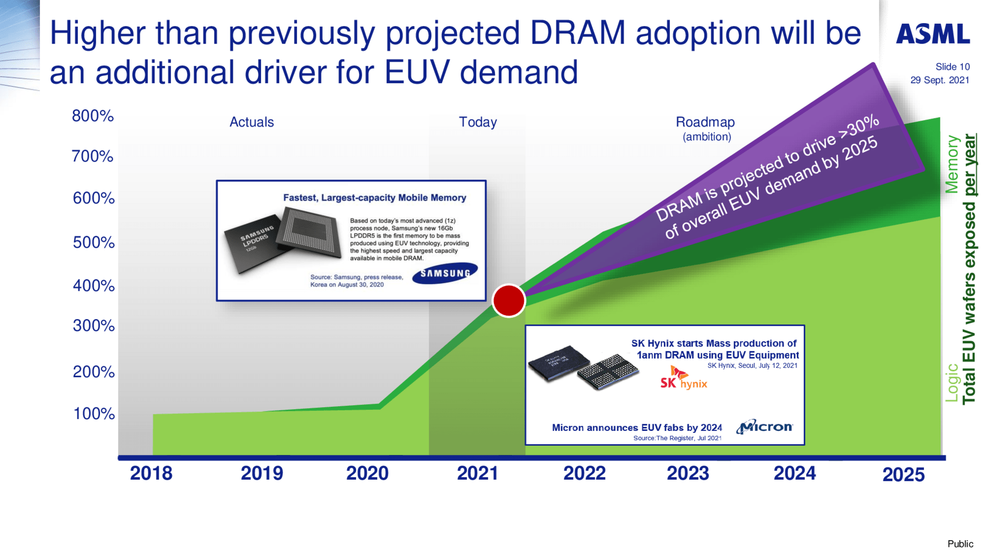
EUV brings Samsung up again in a big way. Far behind TSMC in the logic area, the manufacturer scores points in the DRAM business with experience from other areas and is quite far ahead here, if not even in the lead. Only SK Hynix mixes in a little, but without a lot of experience. Micron will not fully switch to EUV for two years. It is undisputed that there will also be bonuses with DRAM at the end of the day. Samsung mentions an advantage of 20 percent in the energy consumption of the chips alone, and a further 20 percent thanks to the increased packing density for overall productivity.
-
 Advantages of High-NA (Image: ASML)
Image 1 of 3
 Advantages of High-NA
 EUV systems
 Samsung's chips At this level, 16 gigabits are initially as usual, which corresponds to 2 GB, and designed for speeds of up to 7.2 Gbps, which can be achieved by DDR5-7200 in the end. The start of series production, however, took a comparatively long time: Samsung opened the pilot line 1.5 years ago and sent samples. For the near future, the manufacturer is still planning to use 24 gigabit chips in the same manufacturing process in order to be able to meet the requests in the server segment for more memory.