

AMD had already flirted with the announcement of the Ryzen 5000, which had been supplemented by a stacked L3 cache, that the technology would also work well in server CPUs. Rumors spread on Twitter now indicate: Milan will be reissued as Milan X with 768 MB L3 cache, of which 512 MB 3D V cache.
3D V-Cache is already official for Ryzen 5000
It is officially known that AMD will start producing Ryzen 5000 processors this year which not only contain the 32 MB L3 cache exposed to date per 8-core chiplet (CCD), but also an additional 64 MB per CCD. So per CCD there is 32 MB + 64 MB = 96 MB cache, a Ryzen 5000 with 16 cores and thus two CCDs comes to 192 MB in total [2 × (32 MB + 64 MB)].
Milan X achieves 768 MB L3 cache with 8 CCDs
With Milan X, AMD appears to be using the same technology in the near future for an expansion of the Epyc series based on the Milan architecture (chiplet I/O die approach with Zen 3), obviously with an unchanged basis. At the top, based on a 64-core processor with 8 CCDs, 8 × (32 MB + 64 MB) = 768 MB L3 cache are possible.
At least that's what the usually accurate Twitter user ExecutableFix claims and has named four potential Milan X models by name in this context: Epyc 7773X, 7573X, 7473X and 7373X with 64, 32, 24 and 16 cores, respectively. The following table contains these models as well as the other Milan processors available so far.
768 MB L3 from 16 to 64 cores
When looking at the four SKUs, it is noticeable that they should all use the full 768 MB L3 cache, which – if Milan X only turns the Milan architecture upside down – only works if even the 16-core Epyc 7373X processor is still available carries all 8 CCDs, but only two out of eight cores are active per CCD. AMD has already followed this approach with Milan: The F models, like the largest 8 CCD expansion stages, offer the full 256 MB because all eight CCDs can be found on the package – down to the CPU with only 16 of 64 active cores.
This is behind AMD's 3D-V-cache technology
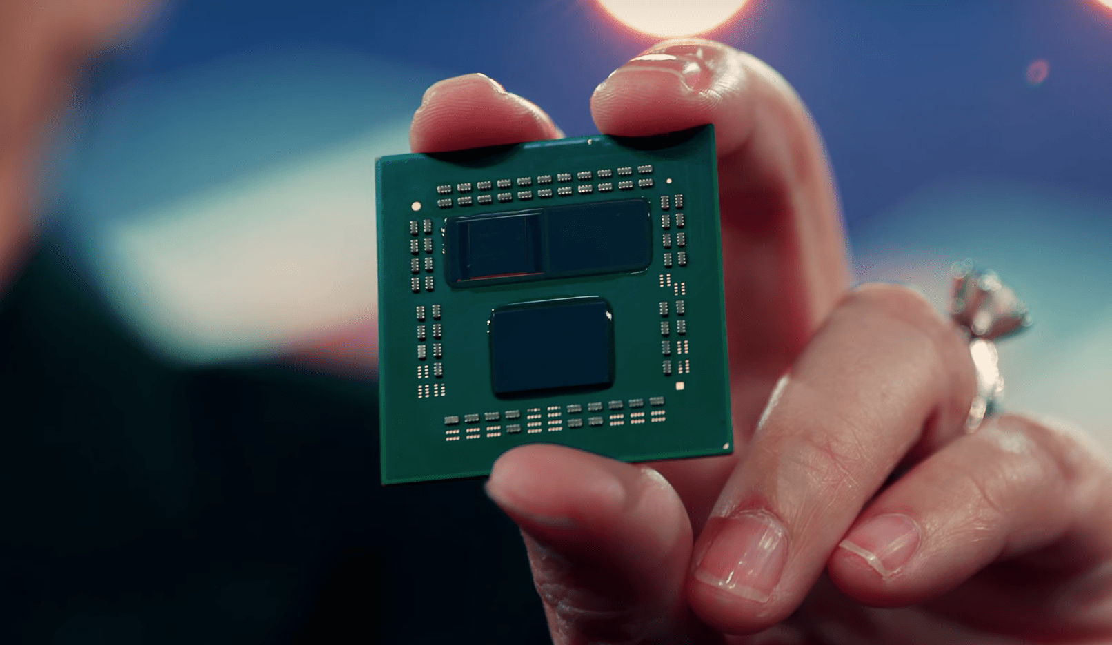
At the presentation of the 3D V-Cache technology at the virtual Computex in June, AMD had already spoken about the technology in detail. The 64 MB additional cache takes up a base area of 6 × 6 mm in the CCD, making it as large as the 32 MB L3 cache that is already in place. With its two 32 MB layers, the new CCD has a triple stacked L3 cache module with 96 MB.
 AMD 3D Chiplet Technology (Image: AMD)
 The attached L3 cache is a native 64 MB chip, it still functions as a direct extension of the existing L3 cache in the CCD, which does not require any software adjustments, as it has no control functions and for all of the units required for the basic functionality can come along. Since these are already in place, AMD can accommodate 64 MB of pure SRAM in the same space as 32 MB before. Zen 3 was already prepared for this possibility from the start, and development and implementation with partner TSMC took several years, AMD explained.
The stacking technology is based on TSVs like them are already used in various stacking solutions. The chip bonding takes place via direct contact of the copper layers, no additional BGA contact areas or the like, such as those provided by Intel's approach with stacking.
In order to use the additional L3 cache on the To accommodate the CCD without changing the height, the CCDs of the relevant processors will be thinner in the future, in order to be just as high as the I/O die in the end with the stacked additional cache and to ultimately fit under the heat spreader.