


Even if the numbers no longer say much about the actual structure width or the progressiveness of a chip, the nanometer race continues. IBM now boasts the first 2 nanometer chip. The new manufacturing process promises major advances in performance and efficiency.
IBM names advantages of 2 nm over 7 nm
Compared to the “currently most advanced 7 nm chips”, the 2 nm process developed by IBM should enable chips with 45 percent higher performance (usually the clock rate is meant) or 75 percent lower power consumption, at least according to the forecast . With which 7 nm process IBM compares here remains open. In the global semiconductor business, the 7 nm processes from the contract manufacturer TSMC are currently in great demand, but Samsung also manufactures in 7 nm. At Intel, the 7 nm process is still pending due to the delays in the 10 nm process. TSMC has been manufacturing the Apple A14 Bionic in 5 nm since last year.
Demand for increased chip performance and energy efficiency continues to rise, especially in the era of hybrid cloud, AI, and the Internet of Things. IBM's new 2 nm chip technology helps advance the state-of-the-art in the semiconductor industry, addressing this growing demand. It is projected to achieve 45 percent higher performance, or 75 percent lower energy use, than today's most advanced 7 nm node chipsi.
iBased on the projected industry standard scaling roadmap
IBM
IBM Research had already developed the first chips at 7 nm and 5 nm, but will not bring commercial products in 7 nm onto the market until later this year in the form of the IBM Power10 processor family. So it will take a long time before the 2-nm chips are mass-produced and other manufacturers could be on the market earlier with similarly manufactured products. The 7 nm chips from IBM are mass-produced by Samsung, so a partnership is also likely for 5 nm and 2 nm. IBM is primarily a semiconductor researcher and less a semiconductor mass producer and only announced a cooperation with Intel in March, which includes the research and development of new technologies.
record-breaking transistor density
While IBM's press release only provides imprecise technical details such as “50 billion transistors the size of a thumbnail”, US media such as AnandTech had the opportunity to find out more information in advance. According to this, the 50 billion transistors are to be accommodated in an area of around 150 mm², which means 333 million transistors per mm² (MTr/mm²). According to the data collected by AnandTech from the Wikichip website, this is a larger transistor density than the estimates for the coming processes 3 nm for TSMC (292.21 MTr/mm²) or 7 nm for Intel (237.18 MTr/mm²). The popular 7 nm process at TSMC is said to be around 91.2 MTr/mm².

A picture from IBM shows the so-called “2nm Nanosheet Devices” under the microscope, each equipped with three Gate-All-Around (GAA) stacked on top of each other. TSMC also wants to use ATM technology from 2 nm, which is superior to conventional FinFET technology. At Samsung, ATM transistors are on the schedule for the coming 3 nm process.
-
 IBM's 2 nm technology at a glance (Image: IBM (via ZDNet))
Image 1 of 3
 IBM's 2 nm technology at a glance
 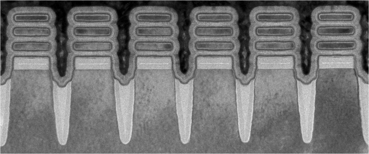 A number of the” 2 nm nanosheet devices “under the microscope
  IBM Research Albany
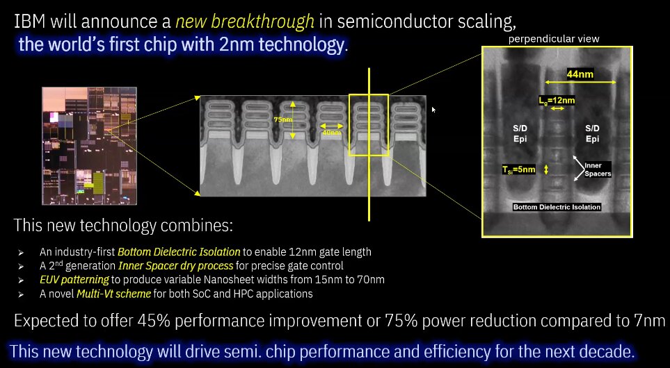
 The “3-stack” GAA cell from IBM's 2 nm chip measures 75 nm in height and 40 nm in the Width, while the gate length is specified as 12 nm and the height of the so-called nanosheets as 5 nm. You will look in vain for structures that measure 2 nm in the IBM film. In the age of 3D transistors, the nanometer designations should rather be understood as an equivalent to a 2D transistor design and give the child a name.
Test chips in the picture, products at the end of 2024
The 2 -nm chips from IBM Research's Albany facility are not yet finished products and are only used to demonstrate the new manufacturing process. AnandTech speculates that these are simplified SRAM chips “with a little logic”.
 Close-up of a wafer with 2 nm chips from IBM Research (Image: IBM)
 As reported by ZDNet, IBM has limited the period for the start of 2 nm series production to the end of 2024. It remains to be seen which semiconductor manufacturer will use the 2 nm process from IBM. It is likely that the 2-nm production will not only be used for the company's own IBM Power and IBM Z systems, as is the licensing of the technology to partners.
IBM has formulated a few more examples of the potential advantages of such chips, such as quadrupling the battery life of cell phones, a drastic reduction in the energy consumption of data centers, faster laptops or faster object detection for self-driving cars. What the chips will ultimately do remains to be seen.