

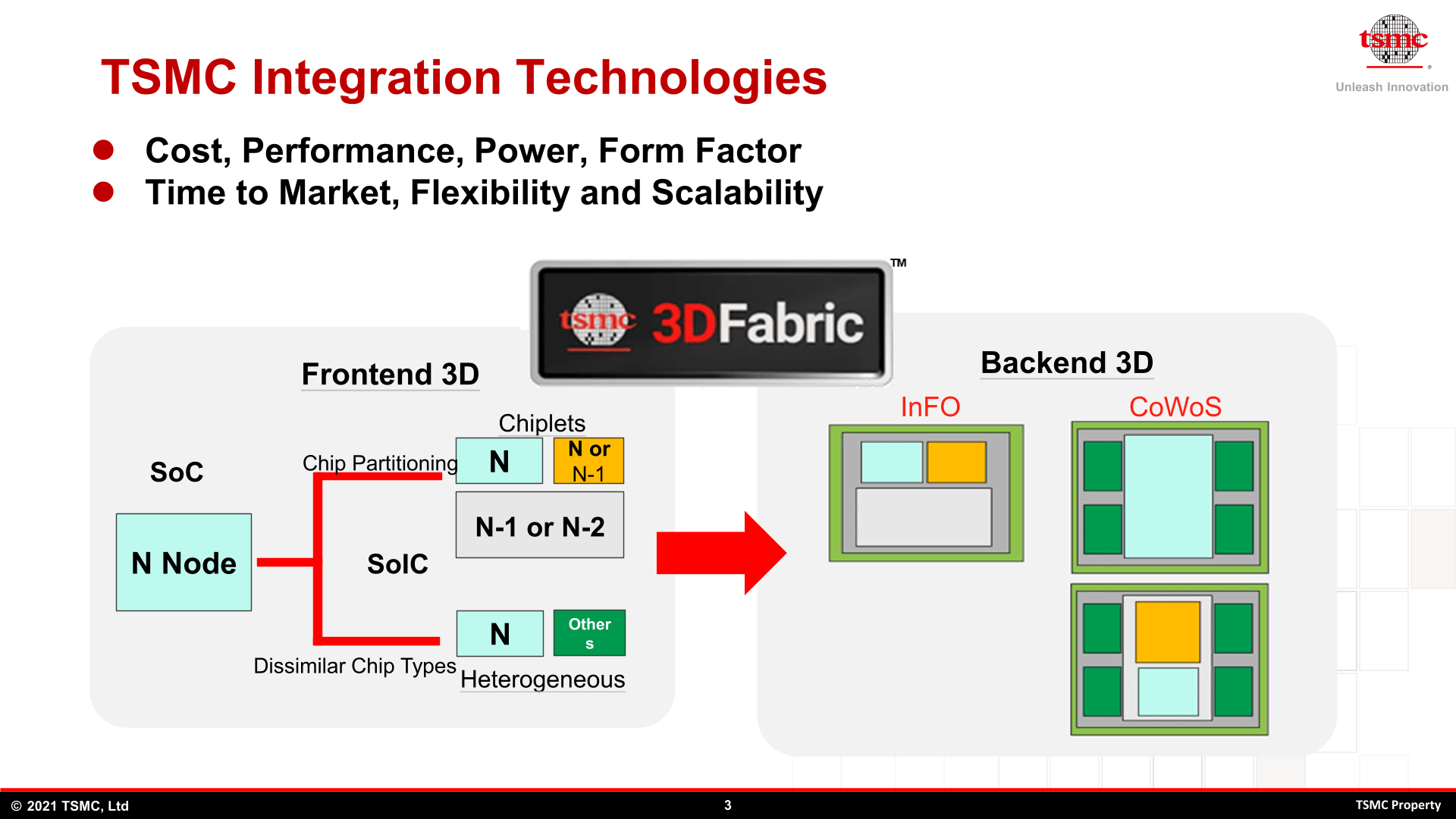
AMD and Intel are talking about market leadership when it comes to packaging, but the real star is TSMC, as they once again demonstrated at Hot Chips 33. Above all, the new 3DFabric, under which the company bundles the modern stacking and packaging processes, is next to InFO and CoWoS the way into the future for TSMC's customers.
TSMC took over an hour as part of Hot Chips 33 to talk about current and future formats only in this market area. Right from the start, TSMC made it clear that these many technologies and code names don't exist to confuse customers. There are special areas of application for each model with advantages that a customer can use.
-
 TSMC Packaging and Technologies (Image: TSMC)
Image 1 of 4
 TSMC Packaging and Technologies
 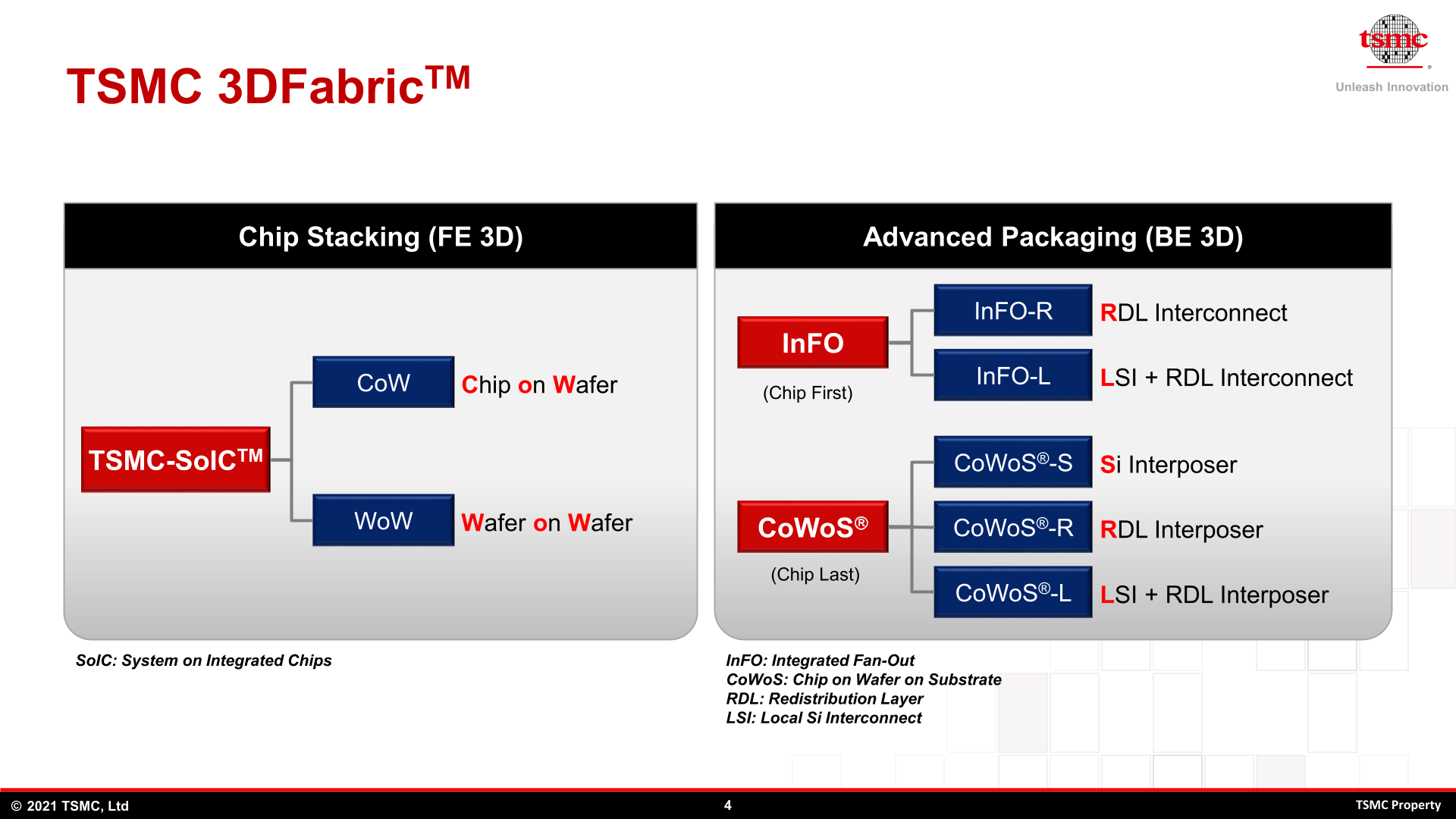 TSMC Packaging and Technologies
  TSMC Packaging and Technologies
 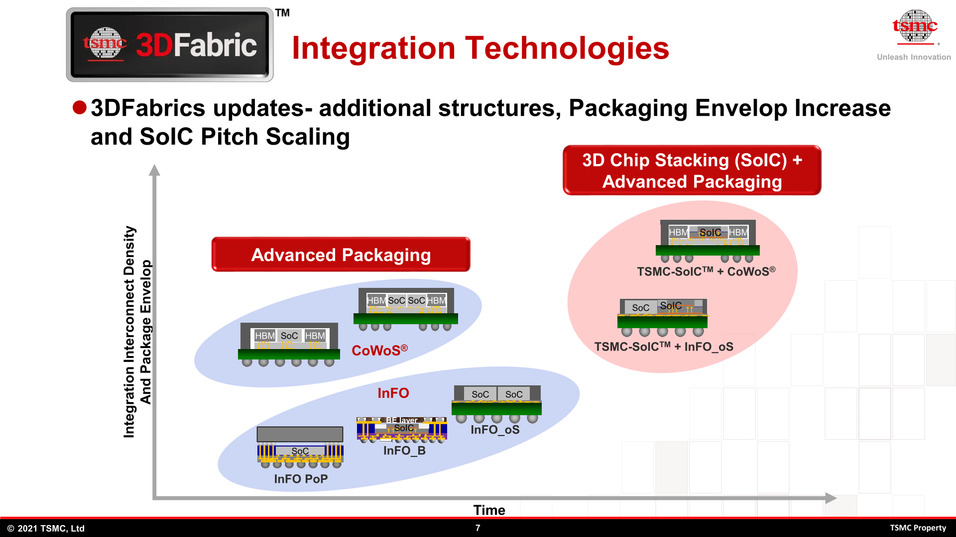 TSMC Packaging and Technologies
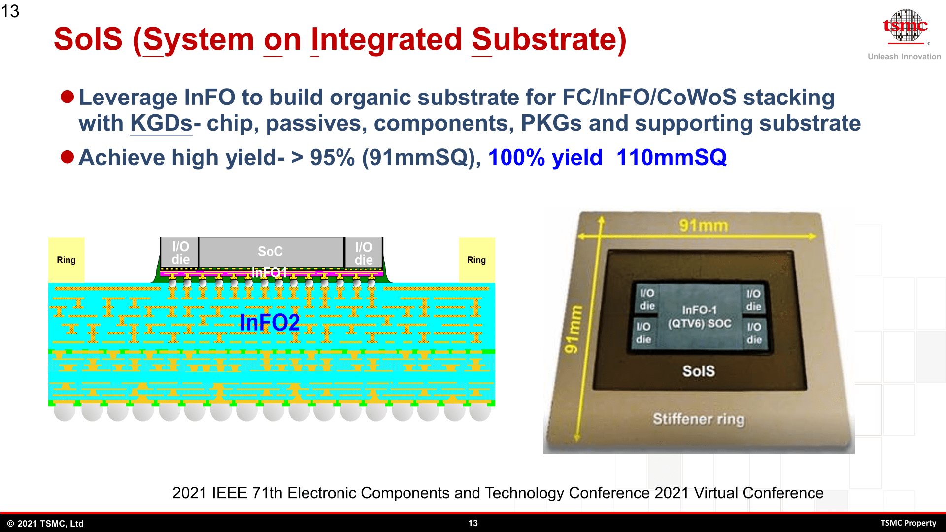
 At the top of the hierarchy, in the HPC segment, many innovations are implemented first. Financial resources are often more generous here, even if the requirements are completely different. Entire systems are implemented here on a wafer, for example, which even offer significant advantages over advanced multi-chip modules. However, they are only suitable for extremely large systems and are therefore still real exotic even in the HPC segment, which have their own requirements for cooling, for example: the right cooling solution can dissipate 7,000 watts – at least in the laboratory so far, TSMC said on request to understand.
-
 TSMC Packaging and Technologies (Image: TSMC)
Image 1 of 7
< figure class = "thumbs thumbs - 7" role = "group">
 TSMC Packaging and Technologies
  TSMC Packaging and Technologies
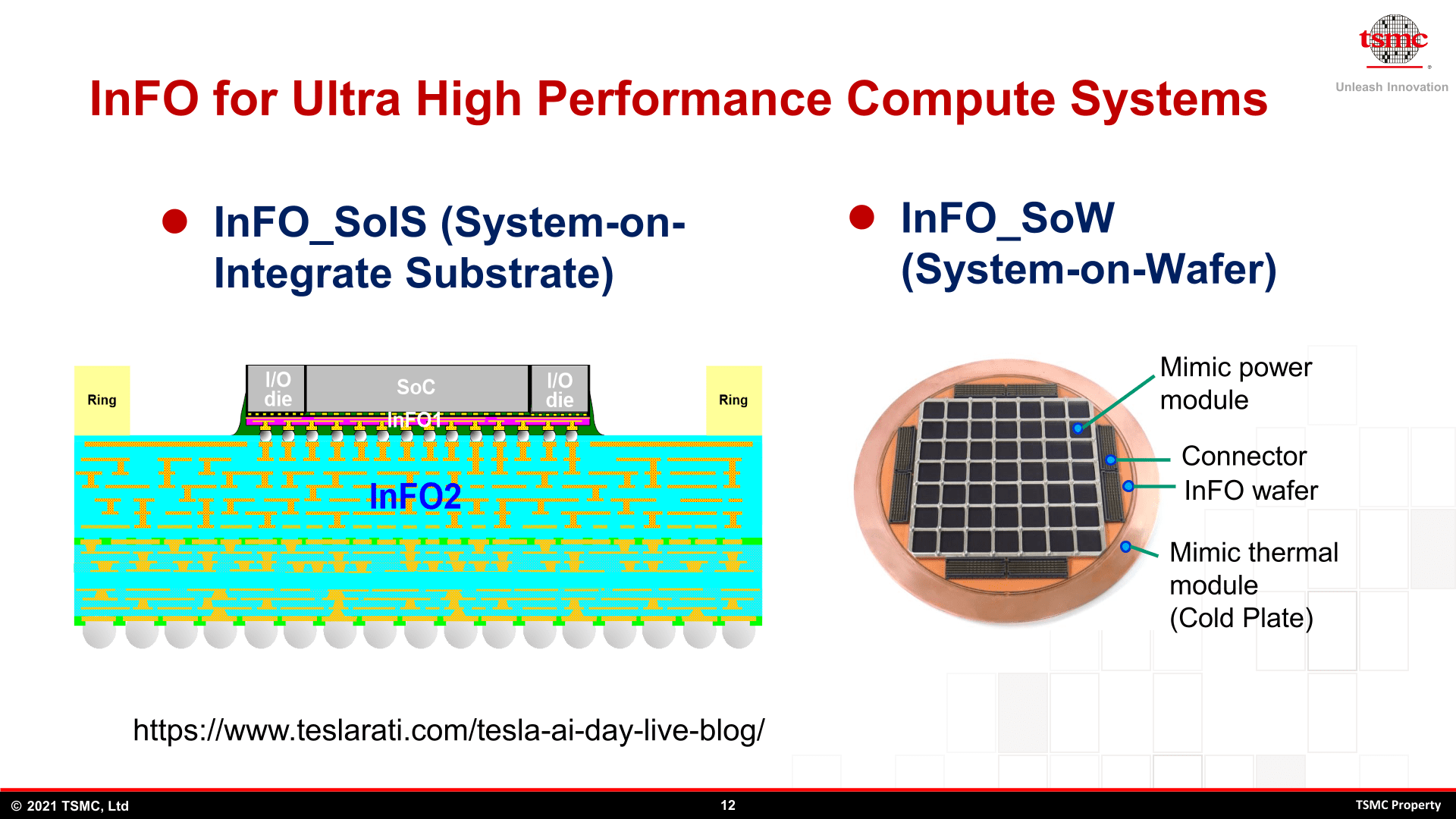
 TSMC Packaging and Technologies
  TSMC Packaging and Technologies
 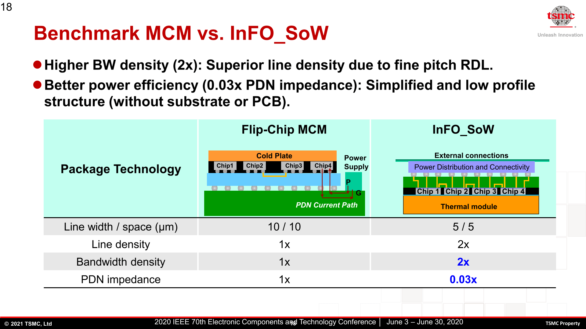 TSMC Packaging and Technologies
 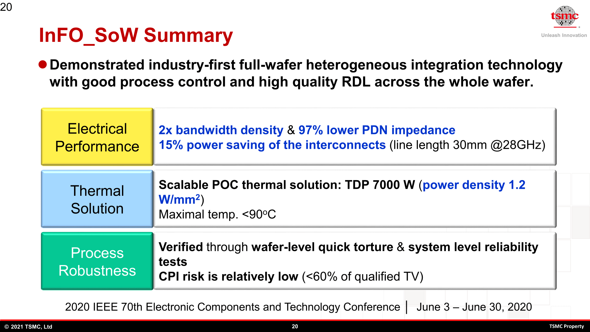 TSMC Packaging and Technologies
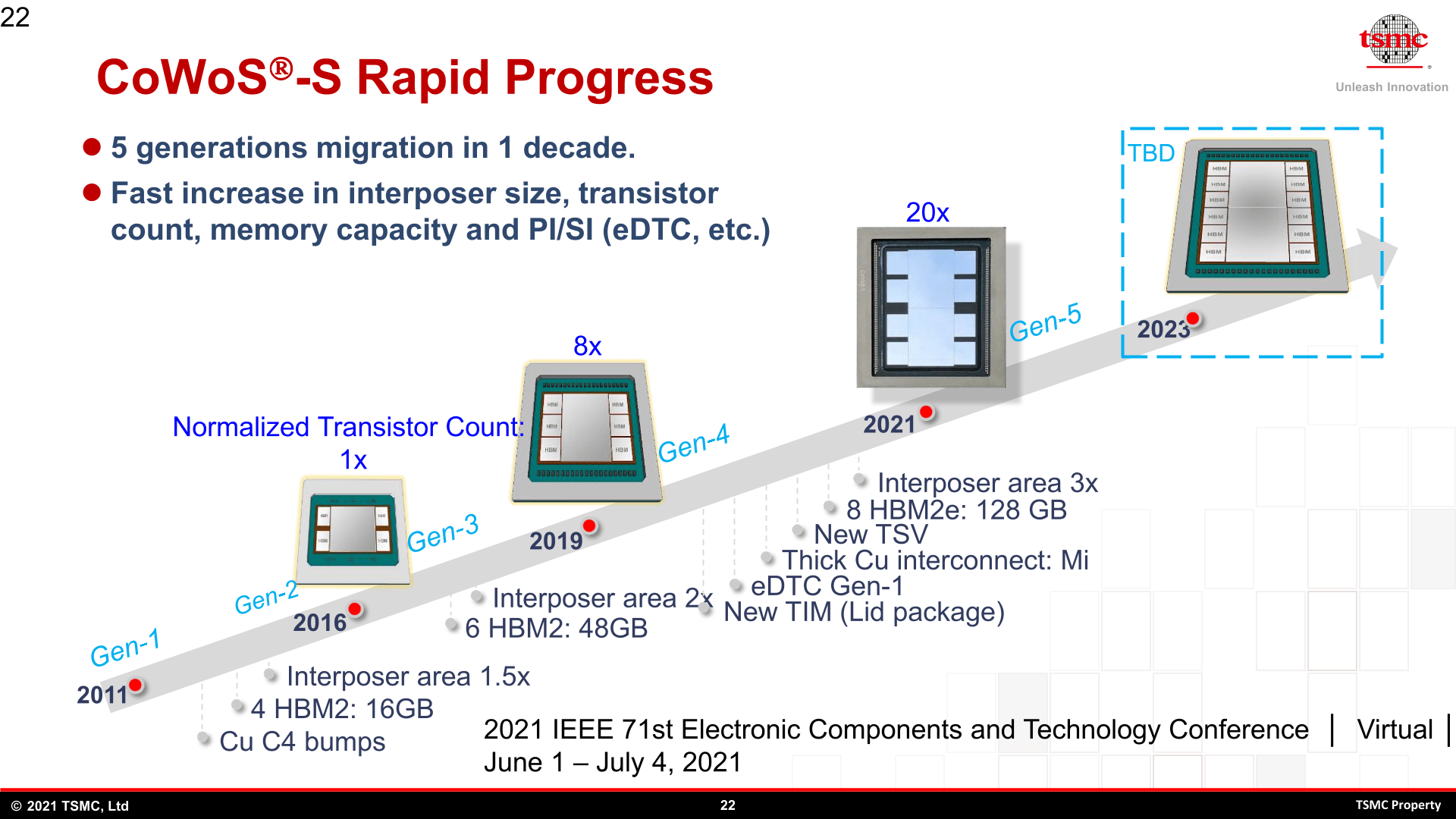
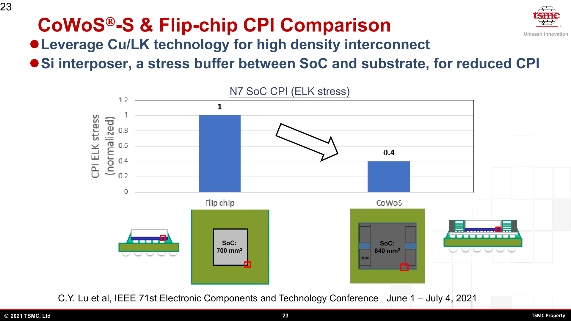
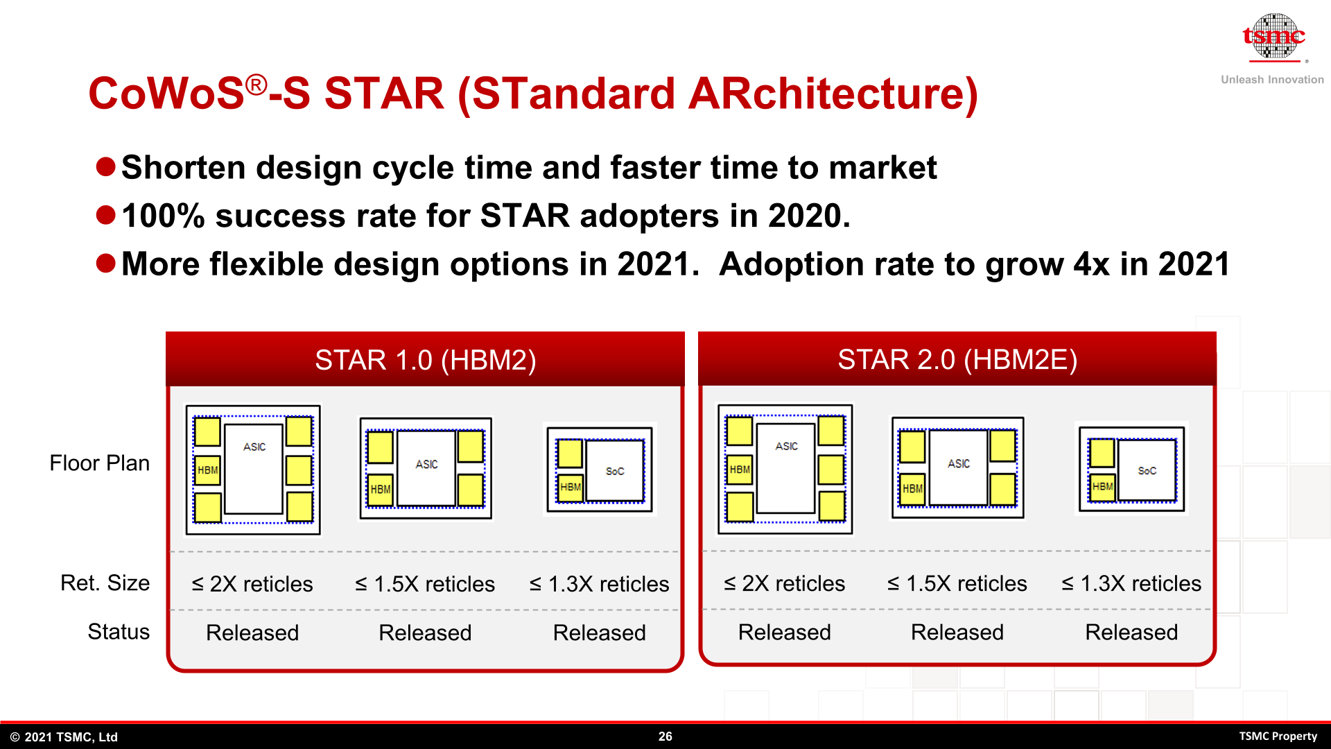
 CoWoS stands for the well-known 2.5D system that has been used for years. In the simplest sense, this is an interposer that is built into the chip along with memory, as has already been seen several times in graphics solutions, for example. A roadmap shows the achievements so far but also the goal of accommodating even more chips on one package. A 2,500 mm² interposer with two large SoCs and 8 HBM chips are the current figurehead, and the number will continue to increase in the future.
-
 TSMC's CoWoS is constantly evolving (Image: TSMC)
Image 1 of 7
 TSMC's CoWoS is constantly evolving
 TSMCs CoWoS is constantly developing
 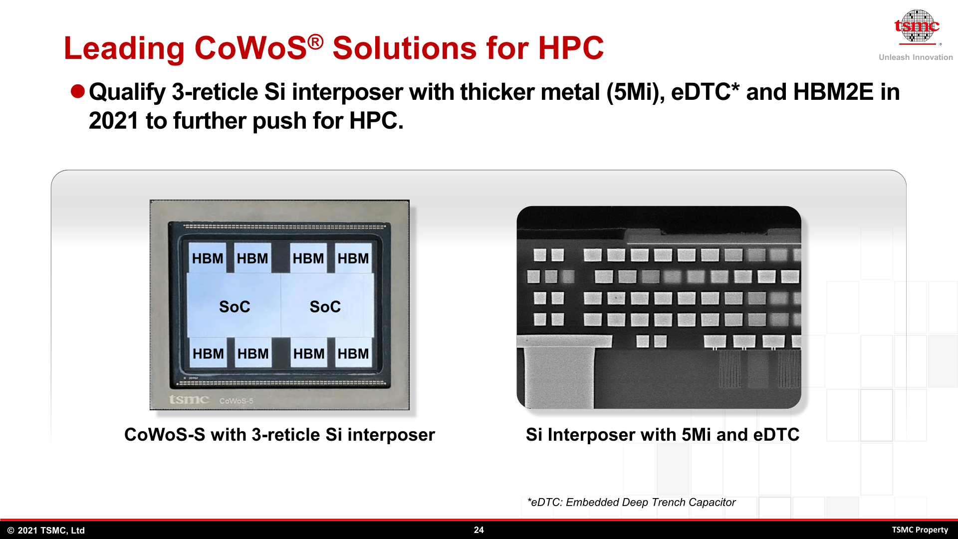 TSMCs CoWoS for HPC
 TSMC Packaging and Technologies
  TSMC Packaging and Technologies
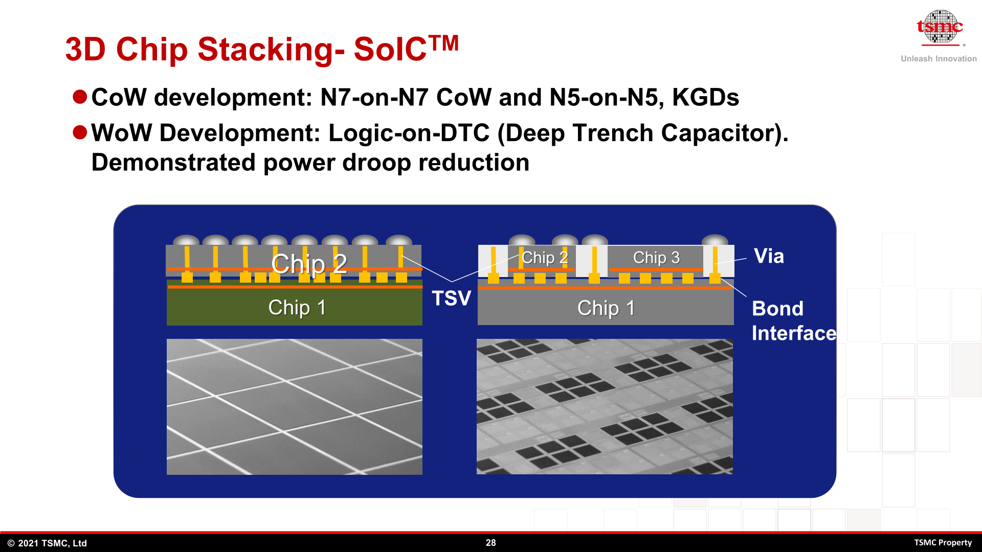
 CoW also includes the first 3D chip stacking solution that AMD will use. A chip made in N7 is placed on top of another chip made in N7. Series production will start at the end of the year, TSMC confirms again, but a short time later N5 will follow N7, but N6 is also explicitly mentioned as a quick intermediate step. Mixtures are not yet planned, but should ultimately also be possible at some point. The roadmap also provides initial indications for the transition to N3. The Wafer on Wafer (WoW) process, however, takes a little longer.
-
 TSMCs 3D Stacking (Image: TSMC)
Image 1 of 2
 TSMCs 3D Stacking
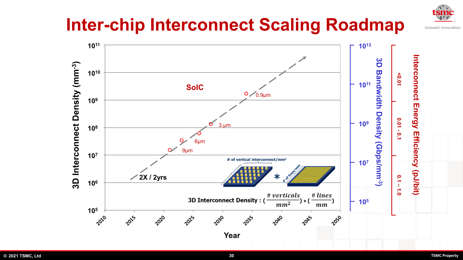
  The scaling roadmap for the small interconnect connections that are required when stacking is interesting. AMD has already announced that the stacked L3 cache in the upcoming Ryzen processors with 3D V-Cache will use connections with a spacing of 9 µm. TSMC's roadmap provides for various reductions down to 0.9 µm – but within more than ten years.
-
 TSMCs Interconnect Scaling Roadmap (Image : TSMC)
Image 1 of 3
 TSMCs Interconnect Scaling Roadmap
  TSMC Packaging and Technologies
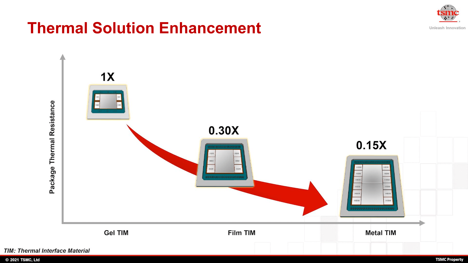
 However, the whole topic of stacking poses challenges for cooling, a topic that Intel also broached for Hot Chips 33. Stacked chips are sometimes difficult to cool; intermediate layers of liquid metal for cooling should help, which lead past as close as possible to the heat source. Compared to direct water cooling in the HPC segment, some of the developments offer great gains in terms of heat dissipation, and in the end the mixture of both is the best.
-
 TSMC's developments in cooling solutions (Image: TSMC)
Image 1 of 2
 TSMCs developments in cooling solutions
  TSMC's developed cooling solutions in comparison
 Silicon Photonics
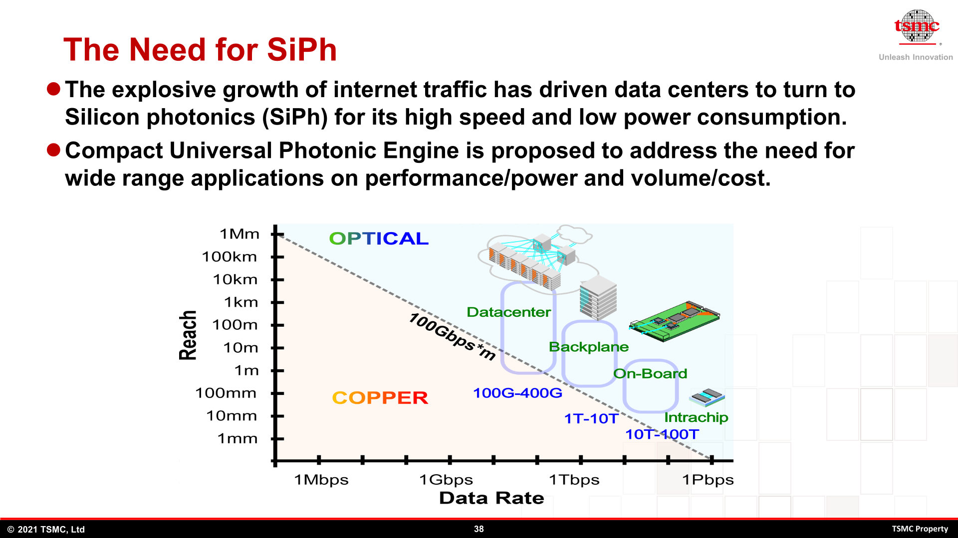
Silicon Photonics is a topic that TSMC also has on the screen. Constantly transferring larger amounts of data with low energy consumption is a challenge for the coming years. The design has already changed in such a way that previously multiple chips have migrated to one package. The aim is to achieve a monolithic design, but due to different technology levels in development, it is often not that far advanced. COUPE becomes TSMC's approach to this. As usual, TSMC does not name customers directly by name, it is up to them to name a partnership themselves.
 TSMC also looks at Silicon Photonics (Image: TSMC)
 Image 1 of 7
 TSMC also takes a look at Silicon Photonics
  TSMC also looks at Silicon Photonics
 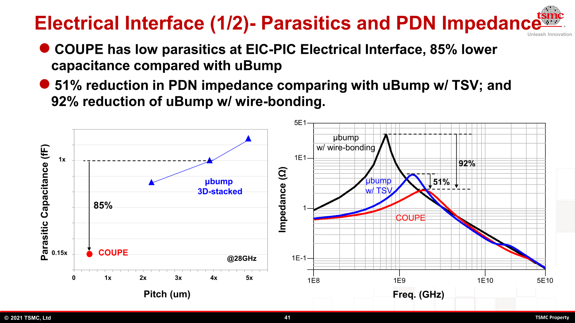 TSMC also looks at Silicon Photonics
  TSMC also looks at Silicon Photonics
  TSMC blic kt also on Silicon Photonics