Two years after the last update, Qualcomm is launching the Snapdragon W5(+) Gen 1 as a new high-end wearable chip. Almost the entire platform has been renewed and switched to 4 nm production. However, the CPU still uses a ten-year-old design. The runtimes should still increase by around 50 percent.
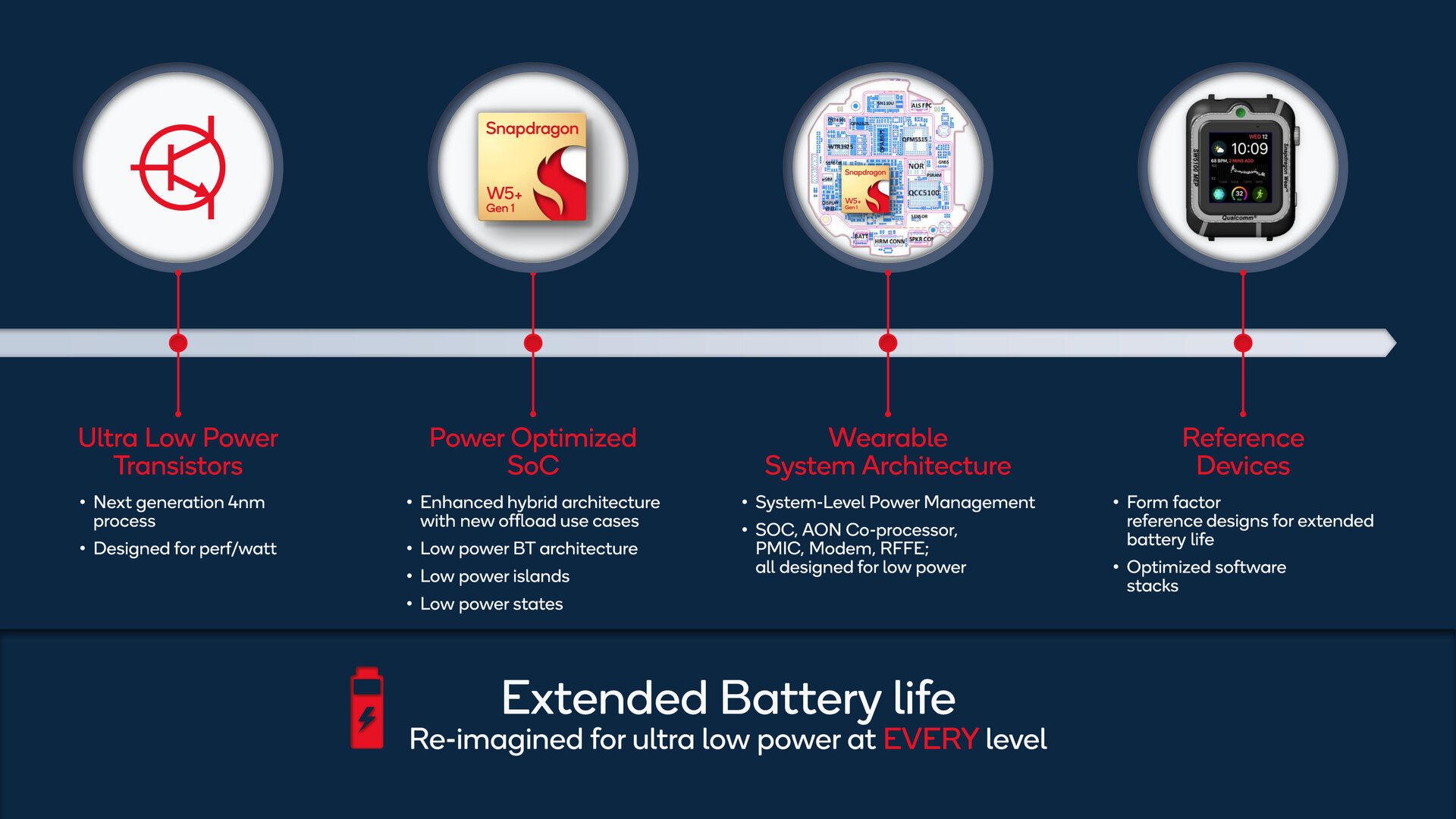
Smartwatch processors are subject to a slower cadence than processors for smartphones. Where Qualcomm presents a new top chip in one segment every year and even in between with upgrades, the processors for wearables are only renewed every two years and with fewer changes so far. However, with the Snapdragon W5+ Gen 1 and W5 Gen 1 taking over the naming scheme of the smartphone chips, the platform is set to experience the biggest changes since the introduction of the first chip in 2016.
Almost all components of W5+ Gen 1 are new
From the Wear 2100 (2016) to the 3100 (2018) and two years ago to the 4100+, there were always only minor adjustments, such as the always-on co-processor, power management IC or production. The W5(+) Gen 1, on the other hand, has a new SoC, always-on co-processor, PMIC, modem and RF front-end, so the entire platform has been redesigned from the ground up. In a preliminary talk, Qualcomm explained that the development of the solution had started about three years ago, before the Wear 4100+ was announced.
-
 Evolution of Qualcomm's wearable platforms (Image: Qualcomm)
Image 1 of 3
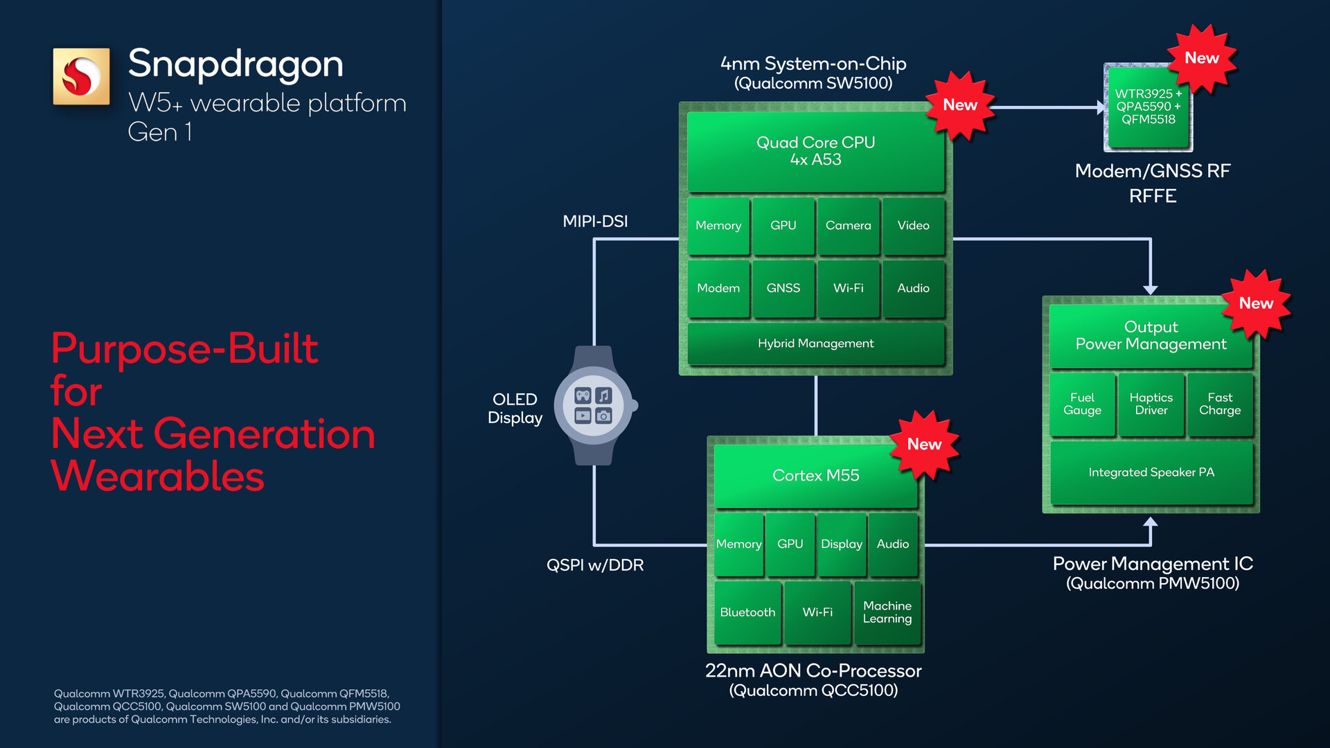 Green indicates the new components of the W5(+) Gen 1 (Image: Qualcomm)
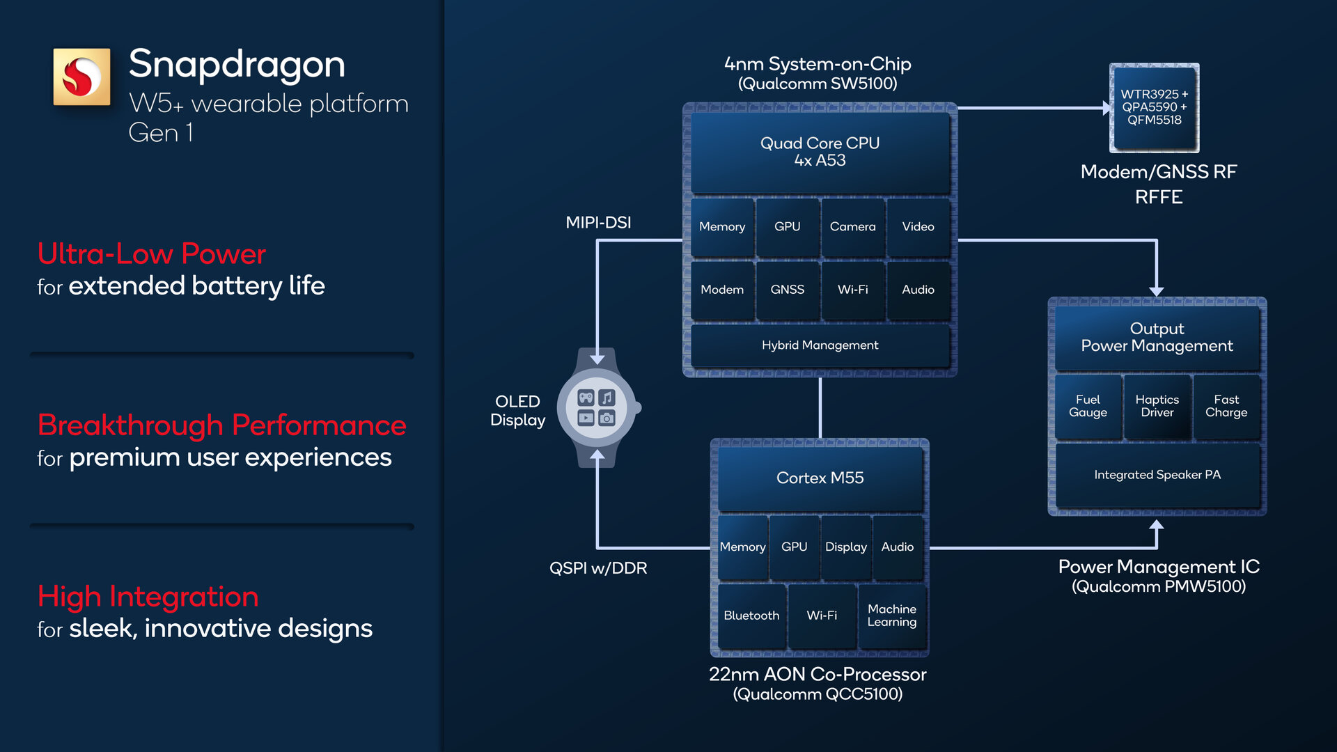
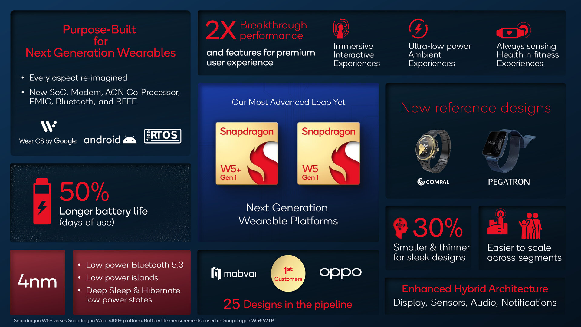 Snapdragon W5(+) Gen 1 overview (Image: Qualcomm)
Always-on co-processor with new arm -Cores
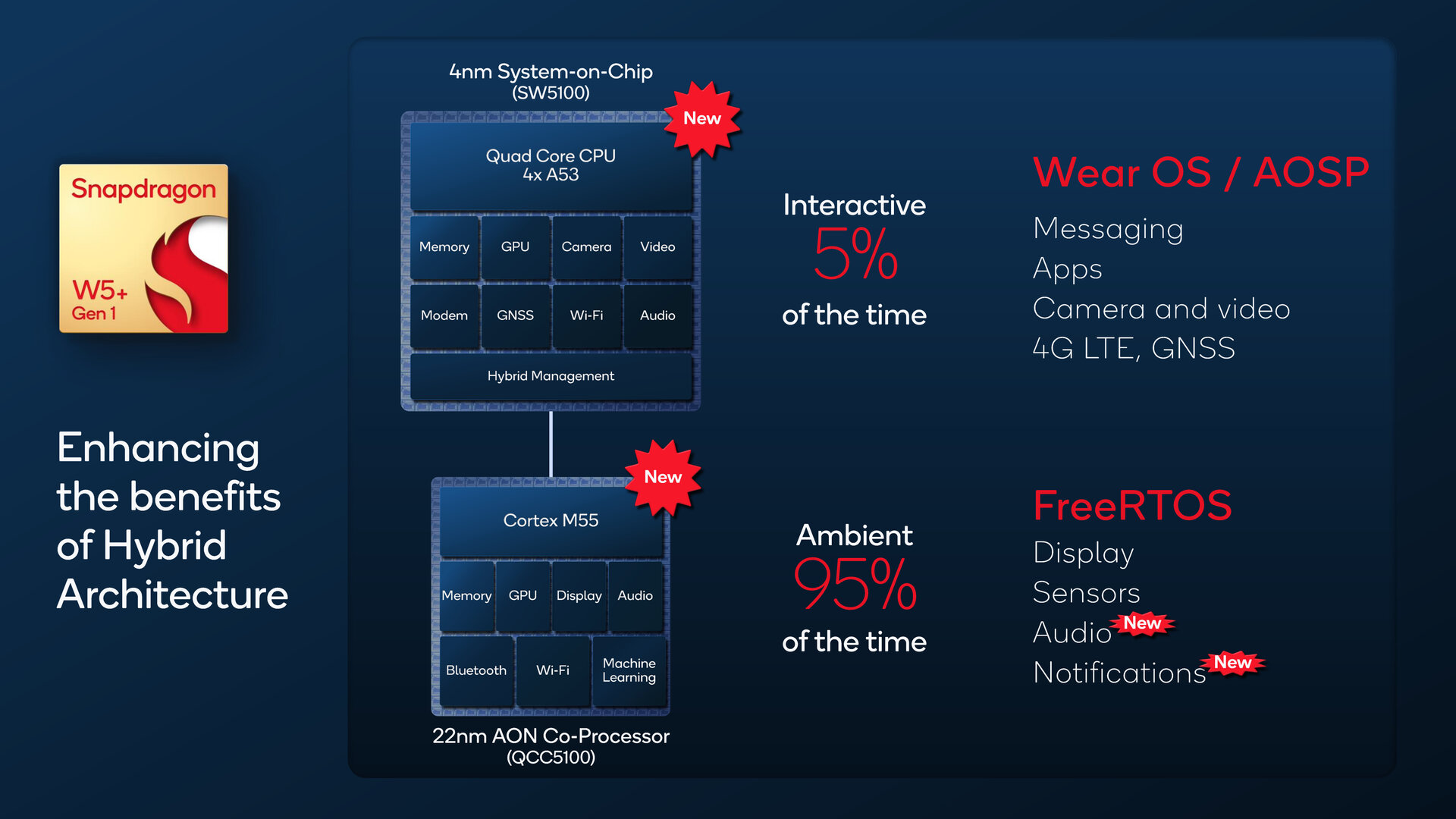
The always-on co-processor, which Qualcomm first introduced in 2018 with the Wear 3100, plays an important role, as according to Qualcomm it is responsible for 95 percent of a smartwatch's tasks that take place in the background. Only 5 percent of the use is made directly with the operating system by the wearer of a smartwatch. The new QCC5100 co-processor has a comparatively modern IoT and NPU core, the Arm Cortex-M55 and Ethos-U55, its own RAM, a GPU, processors for display and audio, Bluetooth 5.3 and Wi-Fi. FreeRTOS runs on the chip as a real-time operating system for embedded systems. The Bluetooth connection to the smartphone is made for the first time by outsourcing this component to the co-processor, which is manufactured for the W5(+) Gen 1 in 22 nm instead of the previous 28 nm.
Main processor uses ten years old Cortex-A53
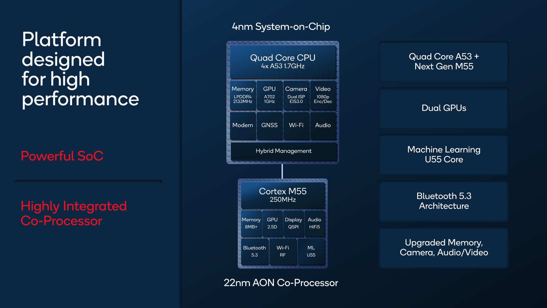
However, the platform also has a main processor for Wear OS or Android with the SW5100. Here is a curiosity, because Qualcomm has decided against using the current Arm IP and continues to rely on a quad-core CPU with up to 1.7 GHz based on the now ten-year-old Cortex-A53 based on Armv8 . In a preliminary discussion, Qualcomm was unable to answer satisfactorily why at least the Cortex-A55 presented in 2017, as used by Samsung in the Exynos W920 of the Galaxy smartwatches, or the Cortex-A510 presented last year is not used. With regard to the Cortex-A55, it was only said that this design would have led to higher consumption in Qualcomm's new wearables platform.
 Structure of the main and always-on co-processor (Image: Qualcomm)
This statement cannot be understood, because Arm itself advertises the Cortex-A55 with 15 percent higher efficiency and 18 percent more performance than the Cortex-A53. Last year's ARMv9-based Cortex-A510 is also said to increase efficiency by another 20 percent and performance by 35 percent. With the current Arm IP, Qualcomm would have received a significantly more economical CPU with much more performance in parallel.
4 nm production for the main processor
The new main processor does not deliver more performance after the Wear 4100+ already ran at 1.7 GHz, but the efficiency is still better, because Qualcomm is switching from 12 to 4 nm production for the main processor. When asked, the company did not want to reveal whether Samsung 4LPE or TSMC N4 was used. Snapdragon 8 Gen 1 and Snapdragon 8+ Gen 1 have recently shown that the Foundry can make a significant difference in terms of efficiency with supposedly the same nodes, where TSMC has a clear lead over Samsung. Irrespective of this, it should be emphasized that Qualcomm has probably ported a ten-year-old CPU core to a current node for the first time in the industry.
- < figure class="gallery__figure">
 Forecast distribution of tasks (Image: Qualcomm)
Image 1 of 5
 Structure of the Snapdragon W5+ Gen 1 (Image: Qualcomm)
 Tasks for the W5100 SoC (Image: Qualcomm)
 Tasks for the always-on co-processor (Image: Qualcomm)
 Sensor technology runs via the always-on co-processor (Image: Qualcomm)
The main processor also has LPDDR4-2133 RAM, Qualcomm's own Adreno 702 GPU with a clock speed of 1 GHz, a dual image processor (ISP) for cameras, a video encoder and decoder for Full HD, the modem for up to 4G/LTE, a block for GNSS, Wi-Fi and audio as well as the hybrid management for the connection to the co-processor. The main processor is used to connect to the RF front end, which has been equipped with more economical components (WTR3925, QPA5590, QFM5518) from the current generation. The new PMW5100 power management IC sits between the main and co-processor. It offers an amplifier for the integrated speaker and is responsible for battery monitoring, haptic feedback and fast charging.
Low Power Island reduces consumption
Qualcomm has created a so-called low-power island especially for the main processor, i.e. an “island” with low energy consumption, which is always active when the chip uses components belonging to the island, such as GNSS, Wi-Fi or audio. The hybrid management then ensures that the remaining function blocks are deactivated and a switch is made to the co-processor. The deep sleep goes one step further, which only uses the co-processor and consumes less than 1 mA when using the RAM. If the content of the RAM is swapped out to the eMMC in hibernate mode, the consumption should drop below 0.5 mA.
-
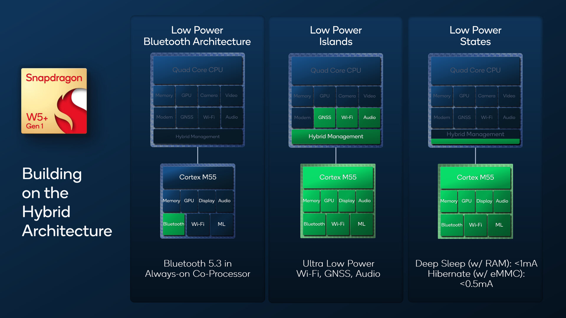 Low Power Island and Low Power State (Image: Qualcomm)
Image 1 of 4
 Measures for extended battery life (Image: Qualcomm)
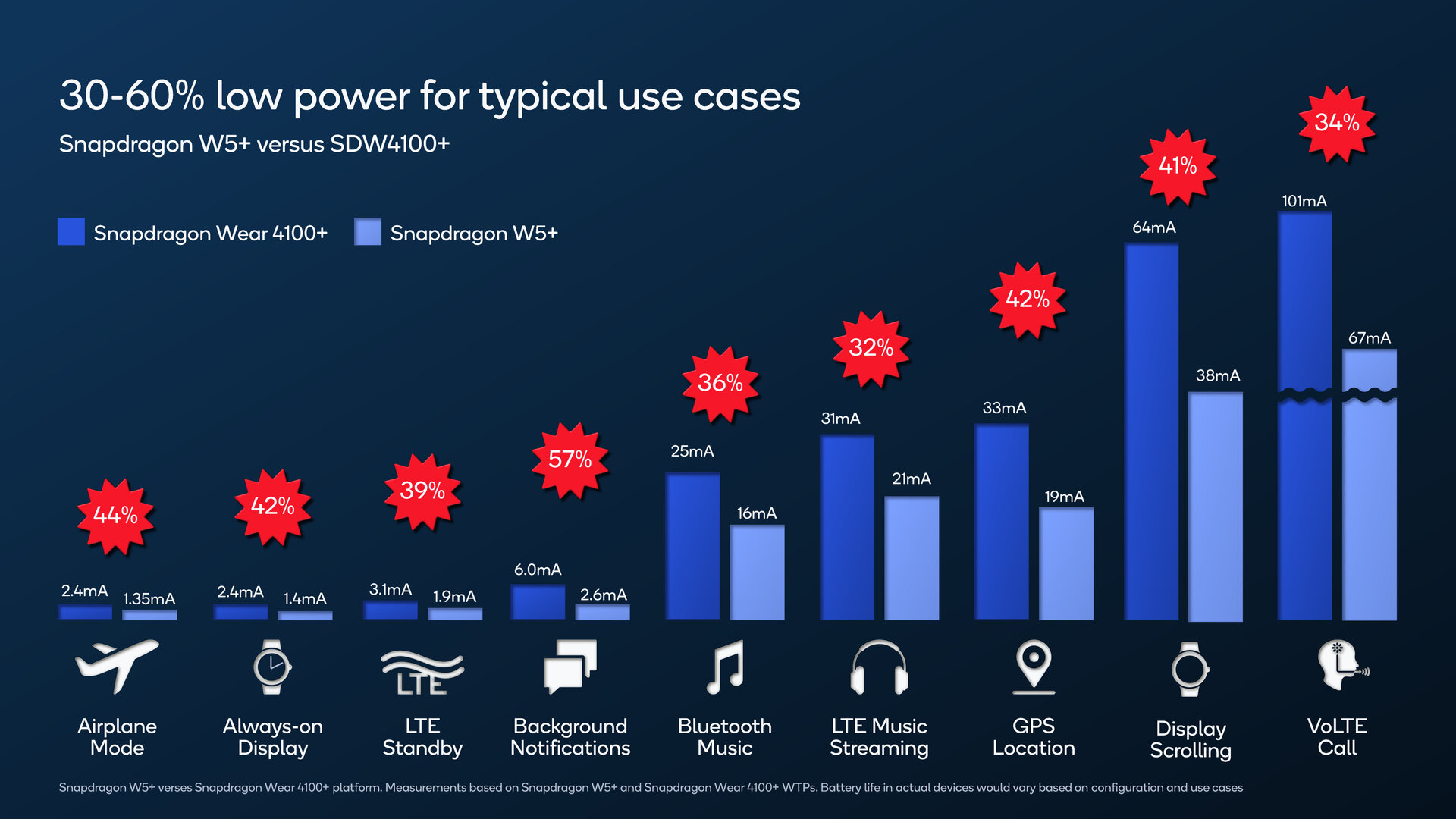 Predicted improvements in battery life (Image: Qualcomm)
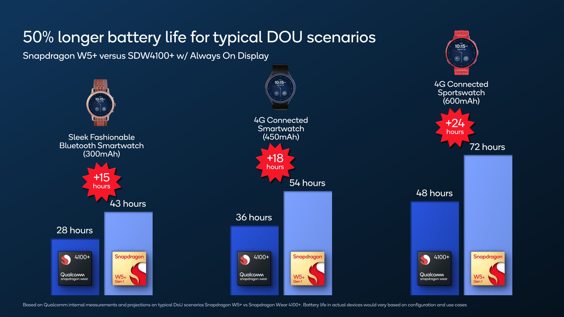 Qualcomm expects 50 percent longer runtimes (image: Qualcomm)
Qualcomm promises 50 percent longer runtimes
It is then primarily the energy consumption that was the focus of the development of the W5+ Gen 1 in particular. Qualcomm developed the W5 Gen 1 without “+” especially for the Chinese market and specific solutions for children, seniors, in the healthcare sector or in the enterprise sector and does without the co-processor in this model. Accordingly, all tasks are assigned to the main processor and the energy balance should be worse, although Qualcomm does not give any figures.
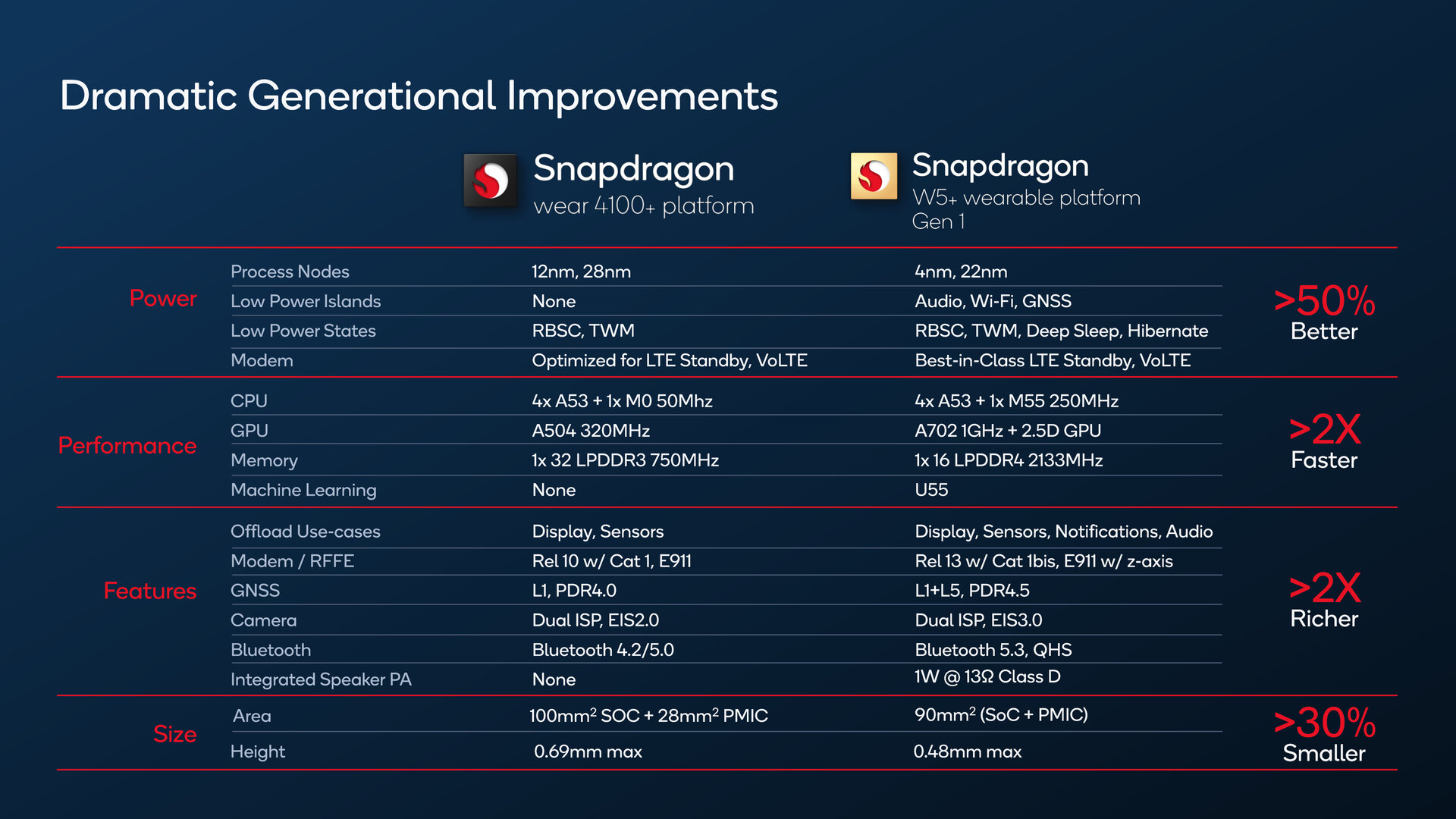
Qualcomm only provides consumption figures for the comparison between W5+ Gen 1 and Wear 4100+. Accordingly, the new platform has significantly lower consumption in all respects, such as airplane mode, always-on display, LTE standby, notifications, Bluetooth music, LTE music streaming, GPS, display operation and VoLTE telephony. Consumption should drop by at least 37 percent, at best by 57 percent, depending on the area of application. Accordingly, Qualcomm promises up to 50 percent longer runtimes for all classes of smartwatches, be it thin fashion products with small batteries, larger LTE smartwatches or sports watches with particularly large batteries.
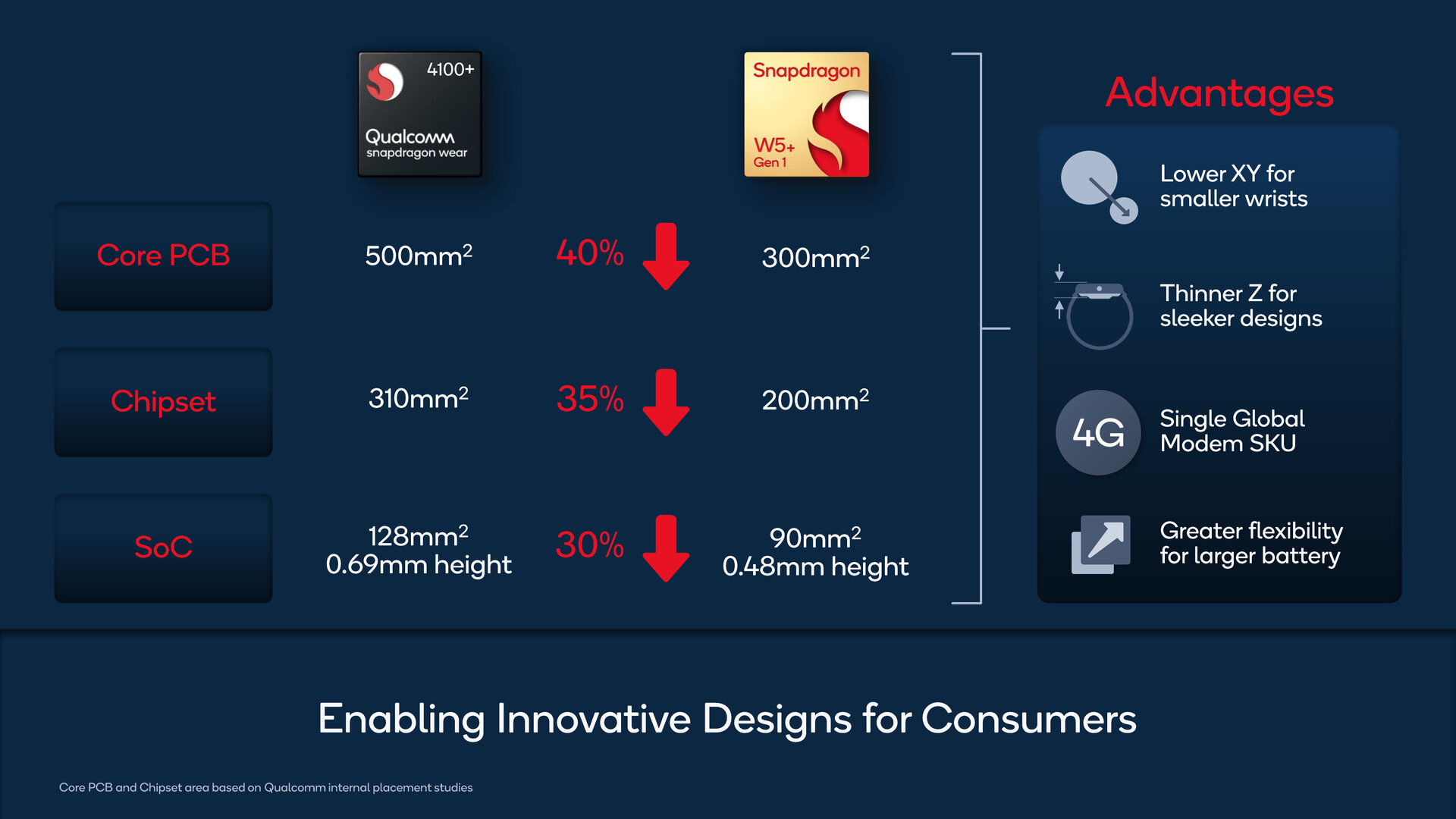
Qualcomm has not only reduced consumption, but also the package of the platform. The core PCB is 300 instead of 500 mm², Qualcomm only mentions 200 instead of 310 mm² for the chipset and the SoC is 90 instead of 128 mm² with a height reduced from 0.69 to 0.48 mm. Manufacturers should be able to develop smaller and lighter smartwatches based on the X, Y and Z axes. In addition, the LTE modem is now always integrated, allowing Qualcomm to work with just one global SKU. It remains to be seen whether every manufacturer will make use of it without a surcharge. And finally, the manufacturers can also install larger batteries in the devices.
-
 Optimizations of the size of individual components (Image: Qualcomm)
Image 1 of 5
 W5+ Gen 1 improvements at a glance (Image: Qualcomm)
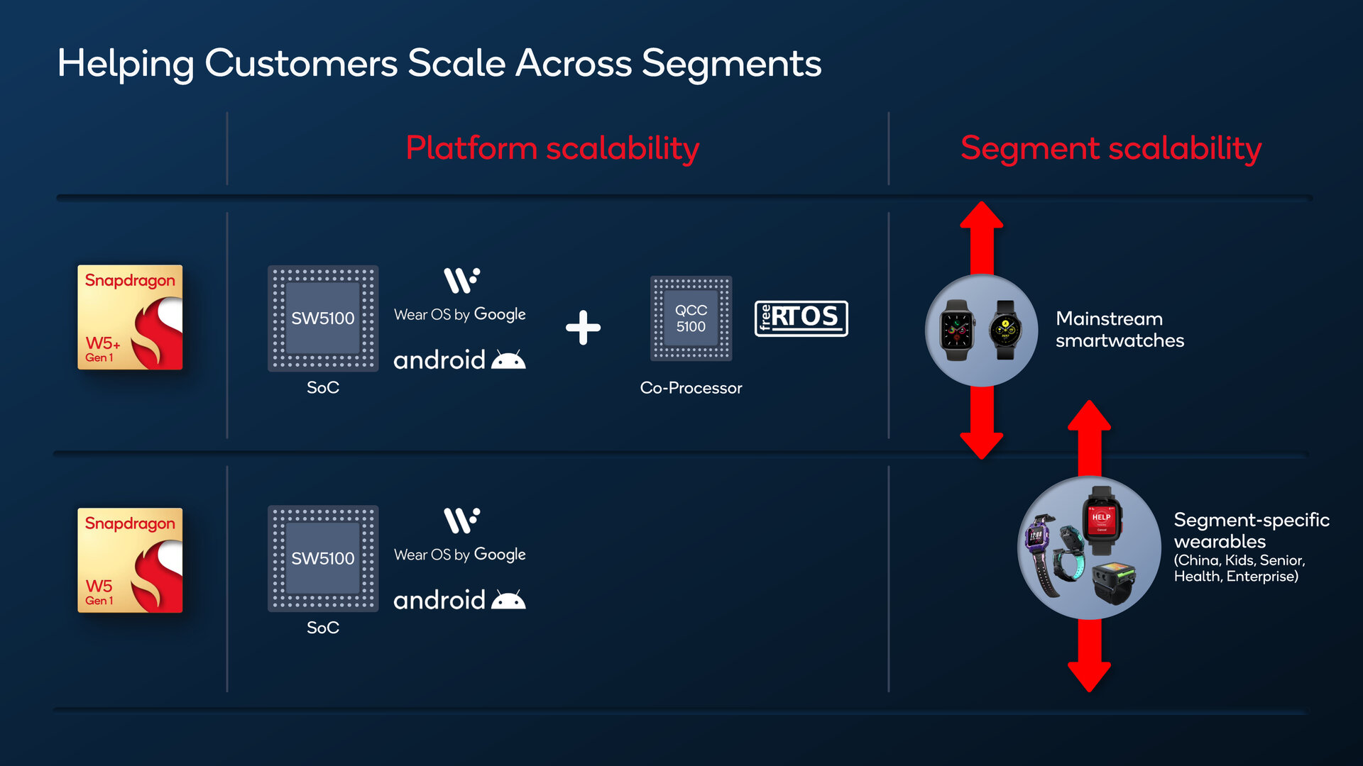 Difference between W5+ Gen 1 and W5 Gen 1 (Image: Qualcomm)
 Support for third-party solutions on the platform (Image: Qualcomm)
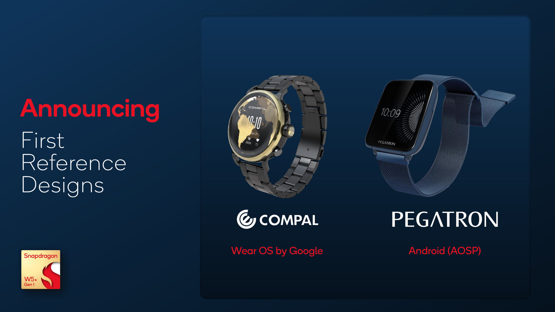 Reference devices running Wear OS and Android (Image: Qualcomm)
First smartwatches from Mobvoi and Oppo
The first vendors of W5+ Gen 1 smartwatches will be Mobvoi and Oppo later in the third quarter, according to Qualcomm. The chip developer also counts 25 other designs from other manufacturers that are said to be in the pipeline.
-
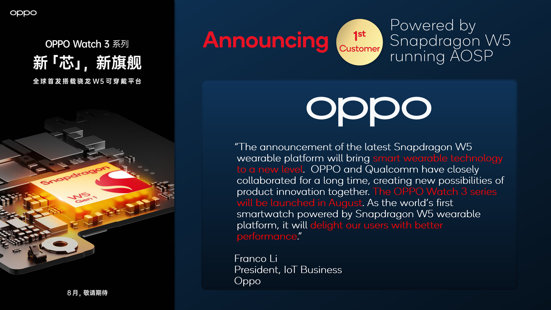 Oppo Watch 3 comes with W5 Gen 1 (Image: Qualcomm)
Image 1 of 3
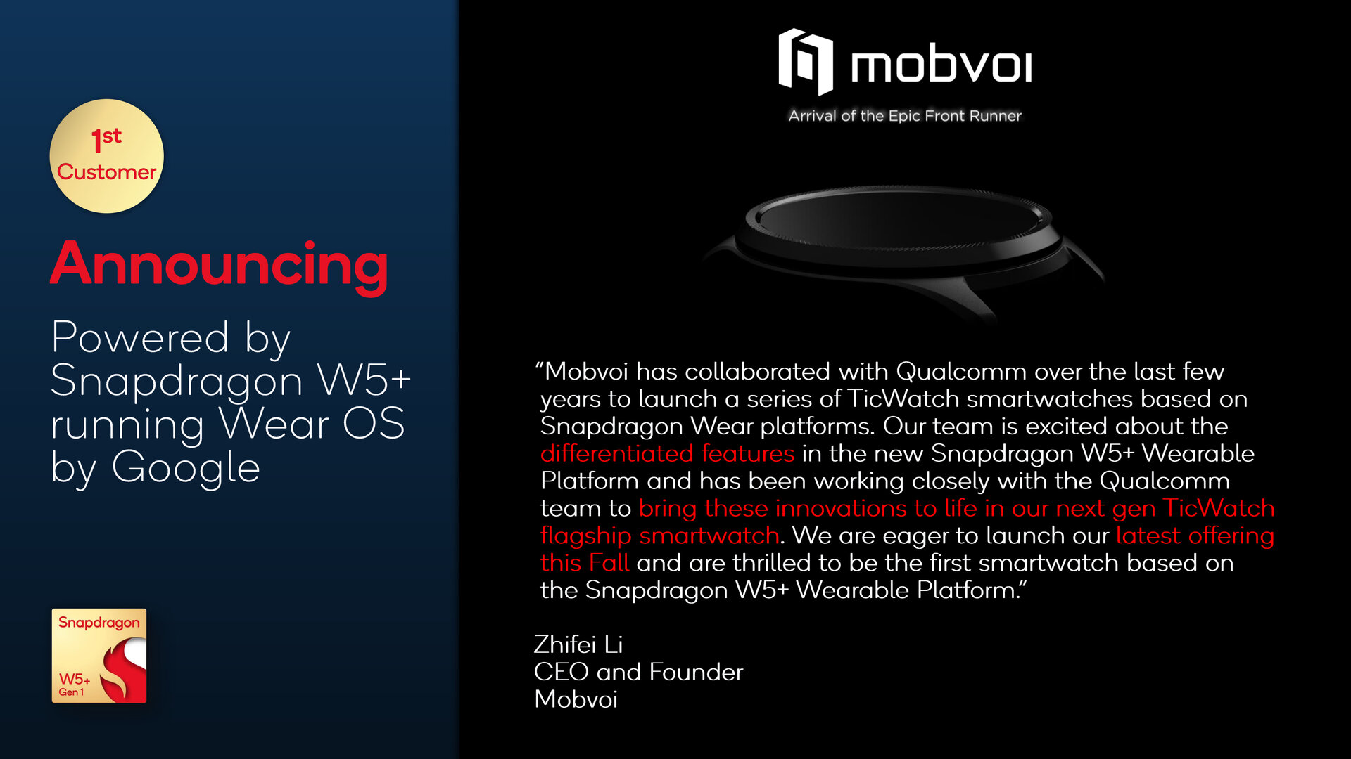 Smartwatch by Mobvoi with W5+ Gen 1 (Image: Qualcomm)< /figure>
 25 more designs in the pipeline (Image: Qualcomm)
ComputerBase has information about this article l received from Qualcomm under NDA. The only specification was the earliest possible publication date.