

The annual International Solid State Circuits Conference continues to provide the first details on the next generation of NAND flash memory. Intel and SK Hynix are promising memory chips that are said to have an areal density of over 20 Gbit/mm² for the first time. The technical implementation is very different.
Intel's PLC-NAND (5 bit) with the greatest area density
According to media reports, Intel presented a PLC memory (penta level cell) with 5 bits per memory cell at the ISSCC 2023, which offers 1.67 terabits of storage space on an area of 73.3 mm² . As far as the editors are aware, this results in the highest areal density for NAND flash to date of 23.3 Gbit/mm².
Storage density of 3D NAND (green: TLC, orange: QLC, red: PLC, blue: SLC)
-
- Intel 192L (PLC, 1.67 Tb)23.3
- SK Hynix V9 >300L (TLC, 1 Tb)20.0″>20 Gb/mm²”
- Kioxia/WD BiCS6 162L (QLC, 1TB)15.1
- YMTC 232L (TLC, 1TB)15.0
- SK Hynix V7 176L (QLC, 1Tb)14.8
- Micron 232L (TLC, 1Tb)14.6
- Intel 144L (QLC, 1Tb)13.8
- Samsung V8 238L (TLC, 1Tb)11.5
- SK Hynix V8 238L (TLC, 1 Tb)11.5not confirmed!
- SK Hynix V7 176L (TLC, 512 Gb)10.8
- Kioxia /WD BiCS6 162L (TLC, 1Tb)10.4
- Intel/Micron 96L (QLC, 1Tb)8.9
- Kioxia/WD BiCS4 96L (QLC, 1.33Tb)8.5
- Samsung V7 176L (TLC, 512Gb)8.5
- YMTC 128L (TLC, 512Gb)8.5
- SK Hynix V5 96L (QLC, 1Tb)8.4
- Kioxia/WD BiCS5 128L (TLC, 512Gb)7.8
- SK Hynix V6 128L (TLC, 512Gb)7.8
- Samsung V5 92L (QLC, 1Tb)7.5
- Intel/Micron 96L (TLC, 512Gb)6.3
- Kioxia/WD BiCS4 96L (TLC, 512Gb)5.9
- Samsung V6 128L (TLC, 512Gb)5.0
- Samsung Z-NAND 48L (SLC, 64 Gb)0.6
- Intel/Micron 3D XPoint (SLC, 128 Gb)0.6no NAND Flash
Unit: Gigabit per mm²
As before, Intel relies on a floating gate architecture and now stacks 192 cell layers (layers) on top of each other. Although the group has meanwhile sold its flash and SSD division to SK Hynix, from which the company Solidigm emerged, which in turn had presented the first SSD with PLC-NAND, research in this segment is apparently also continuing at Intel.
SK Hynix wants to break the 20 Gbit/mm² with 300-layer TLC
SK Hynix also wants to break the 20 Gbit/mm² mark. Instead of packing more bits into the cells, SK Hynix continues to rely on 3 bits (TLC) in combination with significantly more cell layers. The upcoming TLC-NAND should have over 300 layers and thus offer more than 20 Gbit/mm². Storage capacity remains at 1 terabit, which means a much smaller chip.
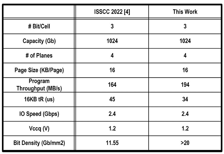
In terms of performance, too, there should be a significant increase. A read latency of only 34 µs and a write throughput at the chip level of 194 MB/s are cited. The soon to be mass-produced 238-layer NAND from SK Hynix, on the other hand, achieves 45 µs and 164 MB/s. Samsung's V7 as the previous leader in writing would be beaten.
< strong>CB-Funk Podcast Episode #11: Annoying account constraints and falling graphics card prices