Shortly before Christmas, AMD's new graphics cards based on RDNA 3 are entering the market. ComputerBase tested the new flagship model Radeon RX 7900 XTX and the Radeon RX 7900 XT, which, among other things, compete against Nvidia's GeForce RTX 4080 and want to score with prices of 1,149 euros and 1,050 euros respectively.
Table of contents < ol class="toc__items toggle-body-container js-toc-items" id="toc">
- RX 7900 XTX and RX 7900 XT for Christmas
- A few words about the technology around Navi 31 and RDNA 3
- The average clock rates under load
- Benchmarks with and without RT in 3,840 × 2,160
- Benchmarks with AMD FSR 2.x and Nvidia DLSS 2.x including ray tracing
- Benchmarks with and without RT in 2,560 × 1,440
- Benchmarks with and without RT in 5,120 × 2,880
- RDNA 3 in current new releases
- Benchmarks in applications
- Volume & ; Cooling
- Power consumption: games, YouTube, desktop
- Energy efficiency in FPS per watt
- Price (RRP) and availability
- Conclusion
RX 7900 XTX and RX 7900 XT for Christmas
AMD's next-gen graphics cards will as announced, hit the retailer shelves before Christmas. As of today, the new flagship model Radeon RX 7900 XTX and the smaller Radeon RX 7900 XT can be tested, from December 13th both the reference design and the first (possibly only a few) custom designs will be available in stores.
And so Nvidia's Ada Lovelace generation now has competition. Probably not the GeForce RTX 4090 (test), which in many respects will remain far unrivaled for AMD's new Radeon RX 7000 series. Instead, the Navi 31 GPU duels with the GeForce RTX 4080 (test), which AMD says it wants to beat in the game grid performance.
AMD wants to score with a lower price
Apart from that, AMD also wants to score in terms of costs, because Nvidia has left a huge barn door open with the previous GeForce RTX 4000 cards. Finally, the GeForce RTX 4080 is undoubtedly very expensive with an RRP of 1,399 euros. The RDNA-3 offshoots will not be a bargain either, but they are cheaper. AMD wants 1,149 euros for the Radeon RX 7900 XTX with 24 GB of memory, the Radeon RX 7900 XT with 20 GB will start from 1,050 euros. Prices are for reference models, most custom designs will cost accordingly more.
RX 7900 XTX & RX 7900 XT vs RTX 4080 – Custom reviews coming very soon
On the following pages, ComputerBase will now test the entire package of the Radeon RX 7900 XTX and Radeon RX 7900 XT and clarify the most important questions. For example, whether ray tracing and thus the vulnerability of RDNA 2 has improved. And what about the energy efficiency of the new graphics cards. Away from the normal test course, the editors also take a look at the latest games such as A Plague Tale: Requiem, The Callisto Protocol and Spider-Man: Miles Morales. Overclocking and undervolting will also play a role. The test will show whether the Radeon RX 7900 XTX will finally be able to beat the Nvidia GeForce RTX 4080.
The article will only deal with AMD's reference design, which will also be available from the board partners apart from AMD itself. Tests of the real custom designs are not yet allowed, but will follow shortly – the first series of tests have already been completed.
- Radeon RX 7900 XT(X): Reference at AMD
- Radeon RX 7900 XT(X): reference and custom designs at Alternate*
- Radeon RX 7900 XT(X): reference and custom designs at Caseking*
- Radeon RX 7900 XT (X): Reference and custom designs at Mindfactory*
- Radeon RX 7900 XT(X): Reference and custom designs at NBB.de*
< h2 class="text-width text-h2" id="abschnitt_ein_paar_worte_zu_technik_rund_um_navi_31_und_rdna_3">A few words about the technology around Navi 31 and RDNA 3
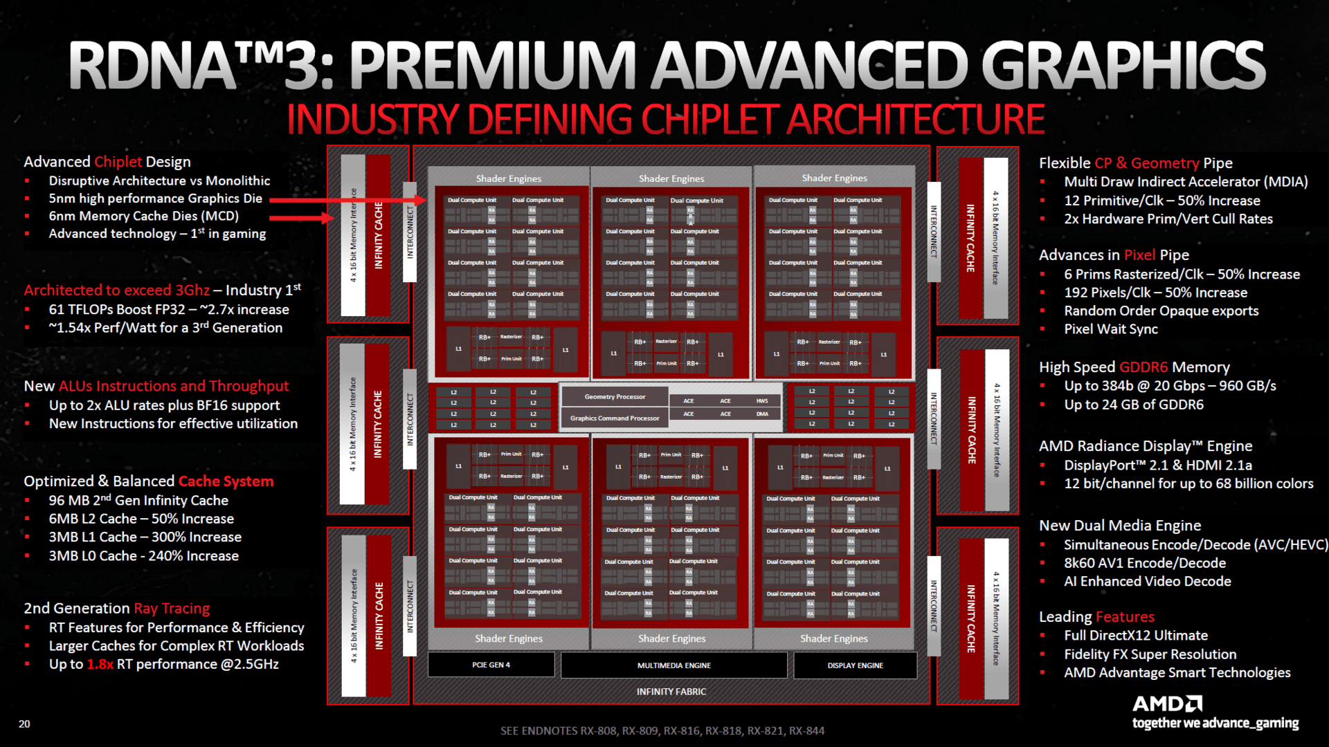
At this point, due to time constraints, the technology of RDNA 3 should not go into great detail, instead only the most interesting innovations are summarized. Navi 31 is the first chiplet design for GPUs that combines a 300 mm “Graphics Compute Die” (GCD) in the N5 process at TSMC with six “Memory Caches” manufactured in the N6 process and measuring a total of 220 mm² Dies” (MCD) combined in one package. According to AMD, this should bring advantages in terms of costs, but also has disadvantages in terms of pure performance.
GPU chiplets have advantages and disadvantages
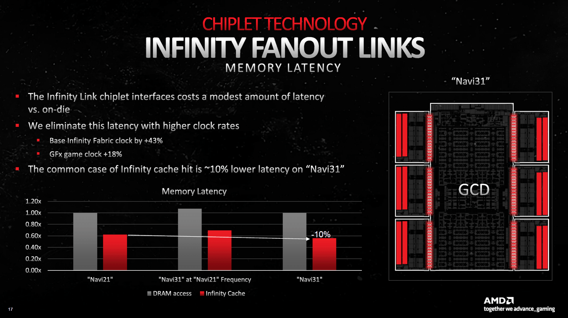
But how are the chiplets actually connected to each other? The “Infinity Fabric” used in the CPUs is not suitable for GPUs, since according to AMD the bandwidth requirement for graphics cards is more than 10 times higher per MCD than for the CPUs per CCD. To make this possible, AMD has developed a new connection called “Infinity Fanout Links” that delivers a total maximum bandwidth of 5.3 TB per second.
However, AMD honestly admits that the chiplet process for CPUs brings cost advantages, but at the same time disadvantages in terms of performance. With the same clock, Navi 21 has a 5 to 10 percent worse latency when accessing DRAM compared to Navi 31. In addition, the latency to the “Infinity Fabric” increases by a comparable value. AMD wants to compensate for this with higher clock rates or even turn it into an advantage, but that doesn't change the fact that a monolithic Navi 31 would still be faster with the same clock rates. This is the disadvantage that GPU chiplets currently have.
-
 Chiplets on Navi 31 (Image: AMD)
Image 1 of 2
 Chiplets on Navi 31 (image: AMD)
Dual issue and more for more power per CU
The GCD consists of a total of 96 compute units in Navi 31 when fully expanded, which is only a small increase compared to the predecessor Navi 21. In order to get a performance increase of more than 20 percent, AMD has now designed the FP32 units as “dual issue”. So you can do two calculations at the same time. Theoretically, this doubles the computing power, with AMD not for nothing refraining from mentioning 12,288 FP32-ALUs (96 CUs × 64 FP32-ALUs × 2) and instead speaking of 6,144 FP32-ALUs.
That is certainly more honest, because AMD has taken the most resource-saving way possible to save transistors. After all, the driver compiler can only combine certain commands, which can then be calculated more quickly. If this is not possible, however, only 6,144 FP32-ALUs are used. Now it's the task of the driver compiler to make as many commands as possible suitable for dual issues – and that's why AMD also says that in the future more programs will be executed twice as fast as they are currently. This means that the driver team also has more work to do with RDNA 3 than with RDNA 2. Nvidia has already taken a very similar path with Ampere with double FP32 units, which goes a little further than AMD's – but probably also costs more transistors.
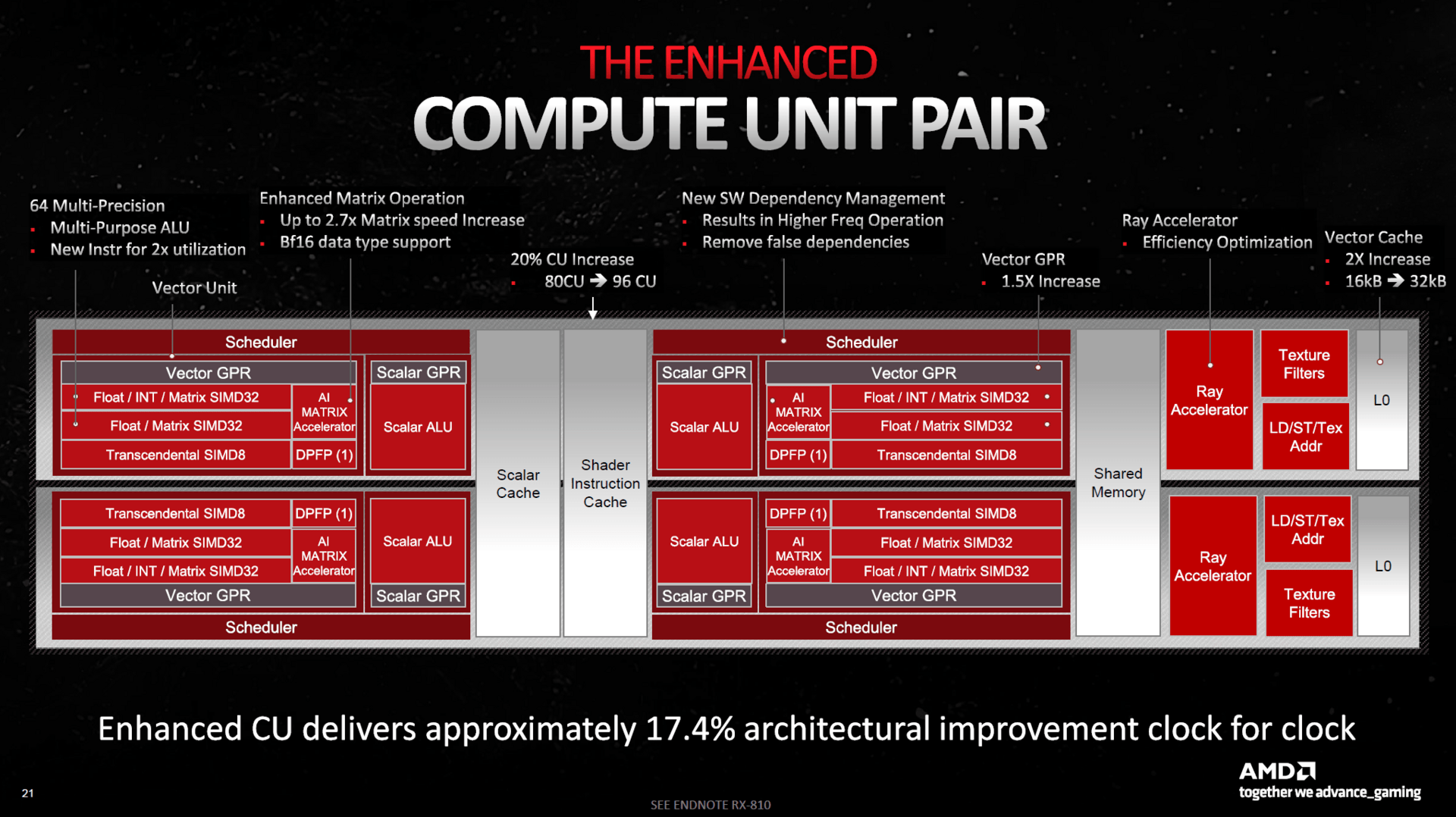
In order to get more performance out of the arithmetic units, AMD has further improved the compute units, although the actual structure has remained the same. The cache sizes have increased significantly, the L2 cache is now 50 percent larger at 6 MB, the L1 cache is 300 percent larger at a total of 3 MB and the L0 cache at 3 MB has also grown by 240 percent. Furthermore, the vector registers have been enlarged and accelerated, so that AMD speaks of an average of 17.4 percent more performance per CU than with RDNA 2 at the same clock rate with RDNA 3.
-
 The architecture of Navi 31 (Image: AMD)
Image 1 of 2
 The architecture of Navi 31 (Image: AMD)
Raytracing makes a big leap, but…
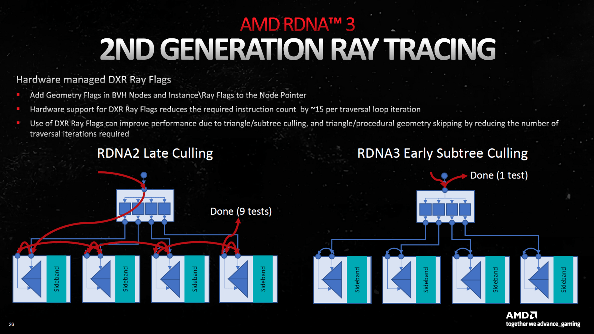
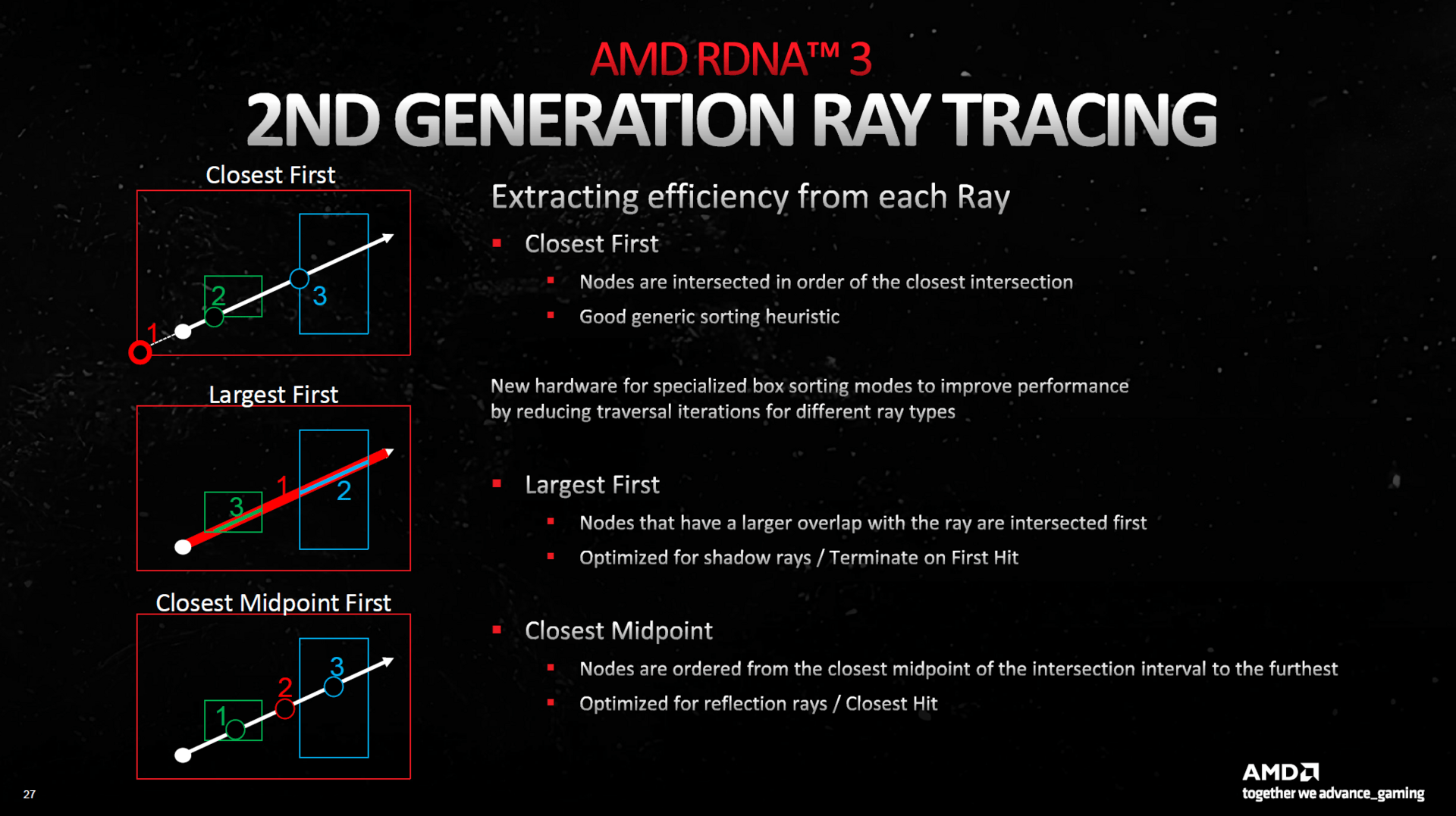
In addition, RDNA 3 introduces the second generation of ray tracing units, which is still structured in the same way as RDNA 2 and is therefore also at home in the texture units – but it should be significantly faster. The RT units of RDNA 2 should no longer have to track every RT ray, but can also cancel those that are no longer needed and, especially in complex scenarios, the “ray tracking” should now work much faster. In general, each individual beam should be able to be guided to the target faster than with RDNA 2. What RDNA 3 still cannot do, however, unlike Nvidia GPUs, is accelerated creation of the BVH structure – this is still done by the FP32 units – and unlike Lovelace, shaders cannot be reordered for optimized ray tracing.
With RDNA 3, AMD speaks of up to 80 percent better RT performance at high RT loads. However, there is one peculiarity to consider here. Like the predecessor, RDNA 3 has one RT unit per compute unit. However, since the number of compute units only increases by 20 percent and the new dual-issue ALUs are no help with ray tracing when the special units limit, the RT performance is up to 80 percent more powerful, at least in theory no disproportionate jump per RT unit. This would have required more RT units per CU. This increases rasterizer and RT performance comparably.
-
 Raytracing at RDNA 3 (Image: AMD )
Image 1 of 3
 < /figure>
Ray tracing with RDNA 3 (Image: AMD)
RDNA 3 with separate KI units – so halfway
A first for RDNA 3 are separate AI accelerators that are a physical part of the GPU on Navi 31. There are 192 of them on Navi 31, so there are 2 of them per compute unit. However, they differ fundamentally from Nvidia's tensor cores and are not nearly as fast. In addition, they don't seem to be able to calculate matrices themselves, but instead can simply prepare for the matrix calculations much faster than before, which in turn are then calculated by the normal FP32 ALUs. Accordingly, the matrix performance on Navi 31 should “only” increase by a factor of 2.7 on RDNA 3. Nvidia mentions significantly higher gains for its own GPUs.
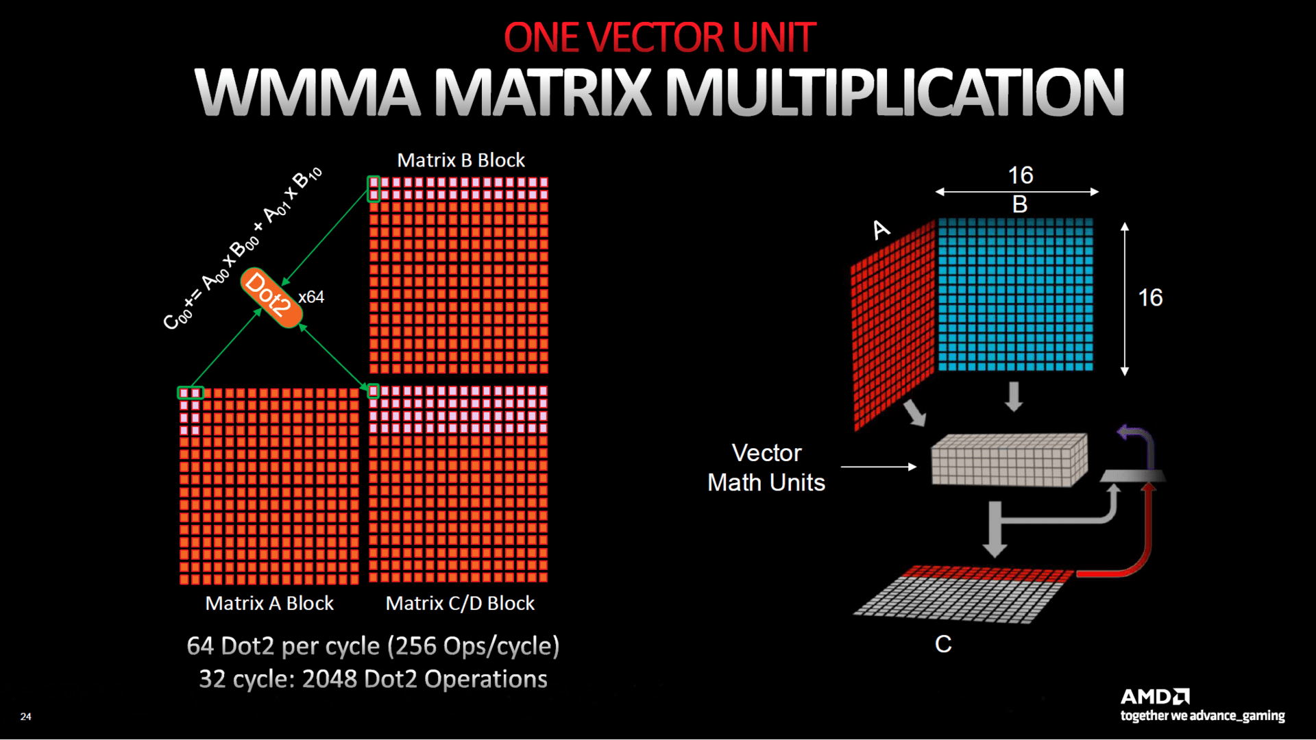 AI units RDNA 3 (Image: AMD)
AMD has expanded the memory interface on Navi 31 from 256 to 384 bits. It is not part of the GCD chip, but is made up of the six MCD chiplets. There are four 16-bit wide memory channels per chiplet, which results in 384 bits on the Radeon RX 7900 XTX with all six chiplets and 320 bits on the Radeon RX 7900 XT with five chiplets (plus a dummy chiplet for better stability of the cooler). The memory expansion increases accordingly to 24 or 20 GB of the GDDR6 type.
Second generation infinity cache is significantly faster
In addition, the second generation of the Infinity cache is on the MCDs, 16 MB of cache are installed per MCD, 96 MB on the flagship and 80 MB on the smaller variant. AMD claims that the Infinity cache has been optimized over the original version so that it has to send data back and forth less often to save energy and thus compensate for the reduced capacity compared to the 128 MB of RDNA 2. In addition, AMD has doubled the performance of the Infinity cache, which contributes a bandwidth of 2.5 TB/s in RDNA 3, while that of RDNA 2 “only” delivered 1.2 TB/s.
1 × GCD + 6 × MCD Chiplet
1 × GCD + 5 × MCD Monolithic Manufacturing TSMC N5 (GCD)
TSMC N6 (MCD) TSMC N7P TSMC N4 Transistors 57.7B 26.8B 45.9B Chip Size 300mm (GCD)
37 mm (1 × MCD) 519 mm² 379 mm² CU/SM 96 84 80 76 FP32 ALUs 6,144/12,288 5,376/10,752 5,120 9,728 RT cores 96, 2nd Gen 84, 2nd Gen 80, 1st Gen 76, 3rd Gen KI- Cores 192, 1st Gen 168, 1st Gen No 304, 4th Gen Tensor Game/Base Clock 2300MHz 2000MHz 2015MHz 2210MHz Boost Clock 2500MHz 2400MHz 2250MHz 2510MHz FP32 Compute Power 61.4 TFLOPS 51.6 TFLOPS 23.0 TFLOPS 48.8 TFLOPS FP16 Compute Power 122.9 TFLOPS 103.2 TFLOPS 46.1 TFLOPS 48.8 TFLOPS Texture Units 384 336 320 304 ROPs 192 128 112 L2 Cache 6,144 KB 4,096 KB 65,536 KBDDR Memory 24 GB GBD DR 66.6 GB 16 GB GDDR6 16 GB GDDR6X Memory Throughput 20 Gbps 16 Gbps 22.4 Gbps Memory Interface 384-bit 320-bit 256-bit Memory Bandwidth 960 GB/s 880 GB/s 512 GB/s 717 GB/s Infinity Cache 96 MB, 2nd Gen 80 MB, 2nd Gen 128 MB, 1st Gen No IC bandwidth 2.5 TB/s 2.0 TB/s 1.2 TB/s No Slot connection PCIe 4.0 ×16 TDP 355 watts 315 watts 300 watts 320 watts
RDNA 3 has two different clock domains
There is still something interesting about the clock rates. Not so with the memory, which works at 20 Gbps, i.e. at 10,000 MHz. With the GPU itself, however, AMD has now divided the “primary clock” into two different clock domains, the front-end clock and the shader clock. On the Radeon RX 7900 XTX, the front end clocks at 2.5 GHz and the actual shader units only at 2.3 GHz. The latter is said to reduce power consumption by up to 25 percent. With the Radeon RX 7900 XT, the clock is 2.0 or 2.2 GHz.
If the graphics card is now overclocked, both domains are increased by the set plus. For example, if you increase the clock by 100 MHz on the Radeon RX 7900 XTX, you get a front-end clock of 2.6 GHz and a shader clock of 2.4 GHz. AMD only passes on the front-end clock to tools (external and in its own driver), the shader clock cannot be read at least currently. As usual, the display is an average value within a certain time frame.
The RX 7900 XT can use a little more energy
Then something about power consumption. The Radeon RX 7900 XTX has a “Typical Board Power” of 355 watts, the Radeon RX 7900 XT one of 315 watts. Anyone who is now concerned about the latter has taken good care, because the Radeon RX 7900 XT was still mentioned as having 300 watts when it was announced. However, AMD claims to have found out in the meantime that the desired performance on all GPUs can only be guaranteed with the additional 15 watts. The manufacturer then decided to go this route instead of minimally reducing the performance. This should not have any effect on other properties of the graphics card.
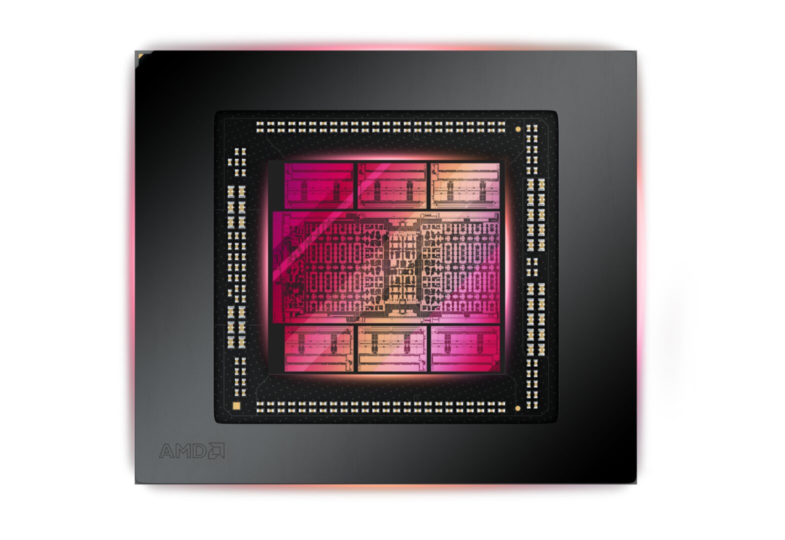 AMD Navi 31 GPU (Picture: AMD)
With DisplayPort 2.1 and AV1 codec
RDNA 3 is the first architecture ever to offer DisplayPort 2.1 in the “UHBR13.5” version as a monitor output. This is not the largest expansion stage, but it still allows a maximum bandwidth of 54 Gbps and thus, with activated DSC compression, for example 4K resolution at 480 Hz, 8K at 165 Hz or WQHD at 900 Hz. In addition, 12-bit color reproduction is possible supported per channel. Corresponding DP 2.1 monitors are expected to appear in early 2023. The built-in USB-C port can also handle the same bandwidth. HDMI 2.1 is also available.
Furthermore, RDNA 3 has a new media engine, or two of them, so that two H.264 or H.265 streams can be encoded or decoded simultaneously. On top of that, RDNA 3 can handle the AV1 codec, here 8K60 or 4K240 is the maximum possible resolution or frame rate. The following table shows more details.
4:2:0, 8 bit 4K210< br>8K48
4:2:0, 8/10 bit 4K240
8K60
4:2:0, 8/10/12 bit 4K210
8K48
4:2:0, 8/10 bit decoding 4K180
4:2:0, 8 bit 4K180
8K48
4:2:0, 8/10 bit 4K240
8K60
4:2:0, 8 /10 bit –
(*) Links marked with an asterisk are affiliate links. In the case of an order via such a link, ComputerBase participates in the sales revenue without increasing the price for the customer.
Page 1/7 Next page
The reference design of the RX 7900 XT( X) in detail