According to a report by Business Korea, Samsung could start producing 3D NAND with a new 236-layer design later this year. In addition, a new center for research and development of upcoming NAND generations is to be opened shortly.
The report from South Korea is scarce and Samsung's plans formulated in it remain unconfirmed for the time being. However, it is to be expected that Samsung will soon be introducing its eighth generation of 3D NAND, also known as V-NAND V8, with more than 200 layers. At its Tech Day last November, Samsung predicted the start of series production of its V8 generation for 2022. Officially there is still only talk of “200+ layers”, Samsung had also promised TLC-NAND with 1 Tbit and revealed that the NAND interface will be further accelerated to 2.4 Gbit/s.
< figure class="text-asset"> TLC 3D-NAND in comparison Micron B58R Kioxia/WD BiCS6 Kioxia/WD BiCS5 Samsung V8 Samsung V7 Samsung V6 SK Hynix V7 SK Hynix V6 Type (bit/cell) TLC (3 bit) Capacity < strong>1 Tb 512 Gb 1 Tb/512 Gb 512 Gb Planes 64 Layer (WL) 232 (2×116) 162 (2×81) 112 (2×56) 200+ (?) 176 (2×88) 128 176 (2×88) 128 ( 2×64) die area ~70 mm² 98 mm² 66 mm² ? ~60 mm² 101.58 mm² ~47 mm² ~66 mm² Density 14.6 Gb/mm² 10.4 Gb/mm² 7.8 Gb/mm² ? 8.5 Gb/mm² 5.0 Gb/mm² 10.8 Gb/mm² 7.8 Gb/mm² Read (tR) ? 50 µs 56 µs ? 40 µs 45 µs 50 µs 56 µs Program ? 160MB/s 132MB/s 164MB/s (?) 184MB/s 82MB/s 168MB/s 132MB/s I/O 2.4Gb/s 2.0Gb/s 1.066Gb/s 2.4Gb/s 2.0Gb/s 1.2Gb/s 1.6Gb/s 1.066Gb/s
< h2 class="text-width text-h2" id="section_a lot of guesswork_about_samsungs_neue_generation">A lot of guesswork about Samsung's new generation
There have already been various statements about the number of layers in Samsung's V8 generation. Business Korea used to report 228 layers, but is now writing 236. An analyst from Techinsights again assumed 238 layers. Ultimately, however, the number of layers is less important than the areal density, performance and durability of the NAND.
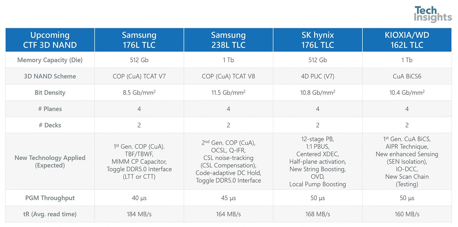 Unconfirmed information about Samsung's “238L” NAND (Image: Techinsights)
If Techinsight's forecast is correct, Samsung would only be able to make a relatively small jump in area density and the performance would even decrease in some cases. Samsung had already confirmed a 4-plane design.
In comparison, Micron's 232-layer NAND performs better in many ways. This achieves by far the highest areal density for TLC-NAND and uses a 6-plane design for even more performance for the first time.
SK Hynix recently finished developing its 238-layer NAND and plans to mass-produce it in the first half of 2023.
Storage density of 3D NAND (green: TLC, orange: QLC, blue: SLC)
-
- Kioxia/WD BiCS6 162L (QLC, 1 Tb)15.1
- SK Hynix V7 176L (QLC, 1 Tb)14.8
- Micron 232L (TLC, 1 Tb)14.6
- SK Hynix V8 (TLC, 512 Gb)14.5not confirmed!
- Intel 144L (QLC, 1Tb)13.8
- SK Hynix V7 176L (TLC, 512Gb)10.8
- Kioxia/WD BiCS6 162L (TLC, 1Tb)10.4
- Intel/Micron 96L (QLC, 1Tb)8.9
- Kioxia /WD BiCS4 96L (QLC, 1.33Tb)8.5
- Samsung V7 176L (TLC, 512Gb)8.5
- YMTC 128L (TLC, 512Gb)8.5
- SK Hynix V5 96L (QLC, 1Tb)8.4
- Kioxia /WD BiCS5 128L (TLC, 512Gb)7.8
- SK Hynix V6 128L (TLC, 512Gb)7.8
- Samsung V5 92L (QLC, 1 Tb)7.5
- Intel/Micron 96L (TLC, 512 Gb)6.3
- Kioxia /WD BiCS4 96L (TLC, 512Gb)5.9
- Samsung V6 128L (TLC, 512Gb)5.0
- Samsung Z-NAND 48L (SLC, 64Gb)0.6
- Intel/Micron 3D XPoint (SLC, 128Gb)0.6no NAND Flash
E unit: gigabits per mm²