

The layer race in 3D NAND is entering the next round. SK Hynix now boasts the highest number of storage tiers in the industry. 238 layers are more than 232 layers at Micron. However, Micron is already in series production, with SK Hynix it will take until next year.
Only SK Hynix speaks of “4D NAND”
Just in time for the start of the Flash Memory Summit 2022, SK Hynix has the announcement of the “World's Highest 238-Layer 4D NAND Flash” ready. The term “4D NAND” comes from the company's marketing department and simply means that in 3D NAND not only the memory cells but also the I/O circuits are stacked in layers on top of each other. This saves expensive chip area and is now common with all NAND manufacturers. But only SK Hynix calls the principle “4D NAND”.
Most layers, smallest chips
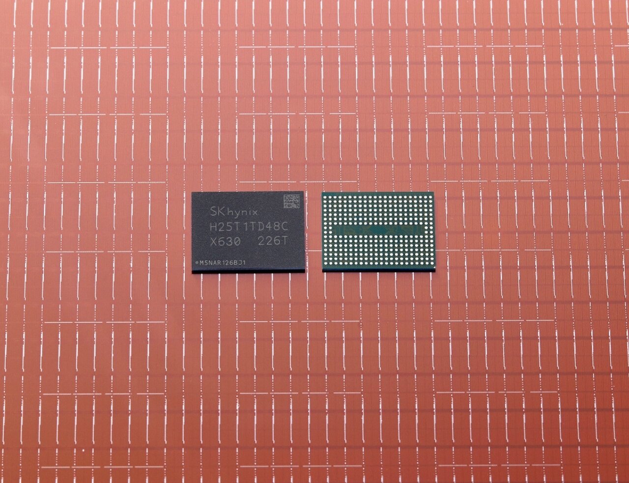
According to SK Hynix, the 238-layer NAND was fully developed in July. Series production is expected to start in the first half of 2023. The memory chips are TLC-NAND with 3 bits per cell and 512 Gbit (64 GB) storage capacity. The 3D NAND should not only be the leader in the number of layers, but also have the smallest area.
It is notable that the latest 238-layer product is most layered and smallest in area at the same time
SK Hynix
The manufacturer speaks of a 34 percent increase in productivity compared to the 176-layer NAND from SK Hynix. If the areal density is meant by that, it would increase from 10.8 Gbit/mm² to around 14.5 Gbit/mm² and the new chip would only measure about a tiny 35 mm². However, this assumption still needs to be confirmed.
Storage density of 3D-NAND (green: TLC, orange: QLC, blue: SLC)
-
- Kioxia/WD BiCS6 162L (QLC, 1Tb)15.1
- SK Hynix V7 176L (QLC, 1TB)14.8
- Micron 232L (TLC, 1TB)14.6
- SK Hynix V8 (TLC, 512 Gb)14.5not confirmed!
- Intel 144L (QLC, 1 Tb)13.8< /li>
- SK Hynix V7 176L (TLC, 512Gb)10.8
- Kioxia/WD BiCS6 162L (TLC, 1Tb)10.4
- Intel/Micron 96L (QLC, 1TB)8.9
- Kioxia/WD BiCS4 96L (QLC, 1.33TB) 8.5
- Samsung V7 176L (TLC, 512 Gb)8.5
- YMTC 128L (TLC, 512 Gb)8.5
- SK Hynix V5 96L (QLC, 1 Tb)8.4
- Kioxia/WD BiCS5 128L (TLC, 512 Gb)7.8
- SK Hynix V6 128L (TLC, 512 Gb)7,8
- Samsung V5 92L (QLC, 1 Tb)7,5
- Intel/Micron 96L (TLC, 512 Gb)6.3
- Kioxia/WD BiCS4 96L (TLC, 512 Gb)5.9
- Samsung V6 128L (TLC, 512 Gb)5.0
- Samsung Z-NAND 48L (SLC, 64 Gb)0.6
- Intel/Micron 3D XPoint (SLC, 128Gb)0.6No NAND Flash
Unit: Gigabits per mm²
Microns 232L-NAND, on the other hand, would be twice as large at around 70 mm², but with 1 terabit per die it offers twice the storage capacity and has an almost identical areal density at 14.6 Gb/mm².
NAND interface accelerated by 50%
So that the growing amounts of data can still be moved quickly, the performance must also increase. Like Micron, SK Hynix uses a NAND interface with 2.4 Gbit/s, which is 50 percent faster than its predecessor. Unlike Micron, however, the manufacturer does not provide any information on the increase in performance when reading and writing. Instead, the equally important topic of efficiency is addressed: the energy required for reading is said to have been reduced by 21 percent.
Client first, 1 Tbit follows
The 238-layer chips from SK Hynix will initially be used for client SSDs and later also for smartphones and server SSDs are used. Next year, SK Hynix also wants to present a variant of the 238-layer NAND with doubled storage capacity of 1 terabit. It remains to be seen whether this is also TLC-NAND or QLC-NAND with 4 bits per cell.