TSMC compensates for the three-year runtime between new nodes with new intermediate stages and more flexibility – even at the transistor level. TSMC calls this approach FinFlex, in which customers can still prioritize between area, performance and energy consumption at a certain production stage. The result is countless possibilities.
N3 nodes in various designs
FinFlex will be based on a TSMC N3 process. Of these, the world's largest contract manufacturer is now planning five variants: N3 as the basic version, which, however, is unlikely to be used. N3E, on the other hand, as an enhanced variant, the focus is fully on this level. This is followed by the classic solution N3P as a performance variant and N3X as an extreme performance version and thus the successor to N4X, which will not be available until next year – which means that N3X is coming late. And right in the middle, N3S is added as a special variant, the exact bonuses of this solution are unclear today, which is why there isn't even a roadmap entry for it.
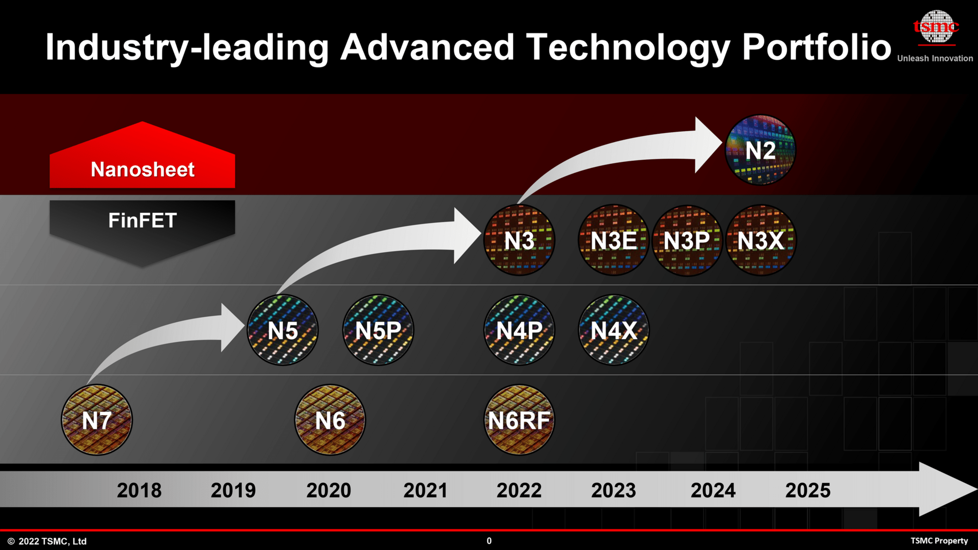 TSMC's roadmap to 2025 (Image: TSMC)
 Interesting are the references of TSMC today. The basic process N3 is not selected in almost any diagram or on a slide, but always goes directly to N3E. It has been rumored for some time that TSMC struggled with the first release, both in terms of bonuses over previous processes and yield. TSMC today emphasizes that the yield is “good” and production will start at the end of the year. However, N3E follows within months with even more performance or lower consumption and improved yields, which suggests that TSMC was not able to implement the plans it originally had – in terms of performance and time. Therefore, N3E is the de facto new basis, also compared to the next big process: N2 based on Nanosheets a.k.a Gate All Around.
 N2 should continue the success story (image: TSMC)
 FinFlex for the best of performance, watts & Area
TSMC also uses this N3E process to explain the new FinFlex implementation. Today's chips are no longer built for just one purpose, but should be able to do many things. The new flexible implementations make it possible to use three different types of transistors on a single die, in order not to use a complete compromise, but to help the respective sub-areas to achieve their best performance or the highest savings.
 FinFlex at TSMC's N3E process (Image: TSMC)
 For example, CPU cores are then manufactured with new 3-2 fins, the middle solution includes a 2-2 fin block, while at the lower end there is a 1-2 fin solution that is fully designed to save power. According to TSMC, this combination also makes it possible to save up to 23 percent in space compared to a solution implemented in the normal way. A common design kit is designed to help customers quickly find and implement the best solution for them. A little video from TSMC explains this a bit.
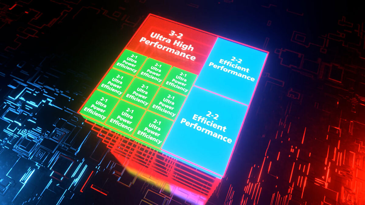 A single die with different fins (Image: TSMC)
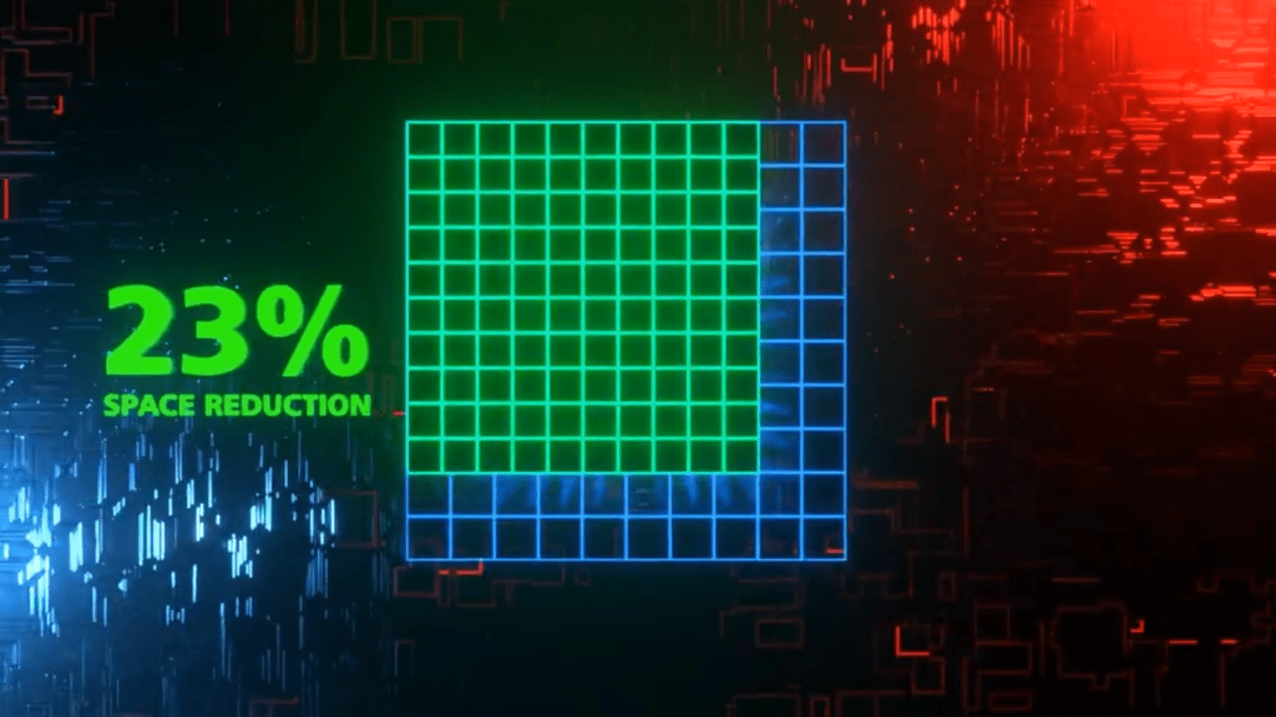 23 percent smaller footprint (Image: TSMC)
< /figure>
Stacked N5 process for 2023 on schedule
TSMC also admitted an update the modern stacking technologies. The media focus is on AMD's 3D V-Cache solution, which will also be used in upcoming Zen 4 processes. These were previously forecast for 2023, TSMC is now declaring that the N5 process will then be ready for these solutions, the newly built 3DFabric factory is scheduled to go into operation almost fully automatically in the second half of this year and will offer significantly more capacity than for the first generation was available. In April, when testing the AMD Ryzen R7 5800X3D with this technology, the editors came to the conclusion that this technology is here to stay.