Nanosheets will play a role at all major semiconductor manufacturers in the future. TSMC also relies on GAA from the N2 production stage, as the world's largest foundry confirms. The technology could be used from 2025. Samsung, in turn, wants to bet on this at 3 nm as early as this year.
Nanosheets go hand in hand with gate all-around transistors
Nanosheets or nanowires are two-dimensional structures with a thickness of less than 100 nm. They have been a topic on the roadmaps and in the research laboratories of the chip industry for years, as they are supposed to make the successor technology to FinFET possible, which uses transistors in a three-dimensional fin structure.< /p>
Nanosheets will be used for the first time with the new gate-all-around (GAA) manufacturing, because it relies on the new thin “threads”. Gate-All-Around is basically very similar to the three-dimensional FinFET that is common today, but with targeted adjustments it should make it possible to jump to below 5 nm.
Further improvement in transistor performance comes from enclosing the last remaining side, the bottom of the channel, with oxide and gate contact as well. This creates a Gate All Around FET or GAAFET. IBM first published this process in 2017.
Samsung is clearly ahead on paper with this technology and wants to deliver the first products this year, while TSMC is only planning to introduce it in the year 2025.
TSMC changes from FinFET to GAA with N2
After all, TSMC has now also confirmed the use of these nanosheets – and thus also that they will switch from FinFETs to GAA technology in the N2 production step. TSMC is considered to be very reserved here, and is still looking for salvation in the classic FinFETS for the upcoming new N3 production stage. There have recently been rumors on this topic that there could be problems with scaling or that the envisaged goals would not be achieved, which TSMC denied. According to TSMC, everything is going according to plan with the new nodes N3 and N3E, production will start in the second half of 2022 in small quantities.
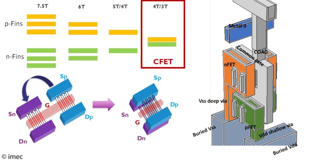 CFET as a possible solution for the future (Image: imec)
 At TSMC, too, nanosheets are only the first step that the manufacturer has to take. TSMC looks further ahead directly to complementary FET (CFET). The stacking of n-type and p-type semiconductors promises a massive reduction in the area required. Many companies have been researching this for years, some in cooperation, and the first lectures were given in 2018. The technology is also very popular at TSMC, but it is also still being researched.
As a bridging until then, fork sheets could take over – the small sheets with the same base look like the tip of a fork lying on its side. Compared to nanosheets, they also promise up to 20 percent less space, ten percent more performance or 24 percent less energy consumption. Since they are seen as an evolution of nanosheets, they should be feasible with slight adjustments. Ultimately, TSMC's developments follow the path that imec has been describing for a number of years.
-
 Forksheet as intermediate step from Nanosheet to CFET (Image: imec)
Image 1 of 2
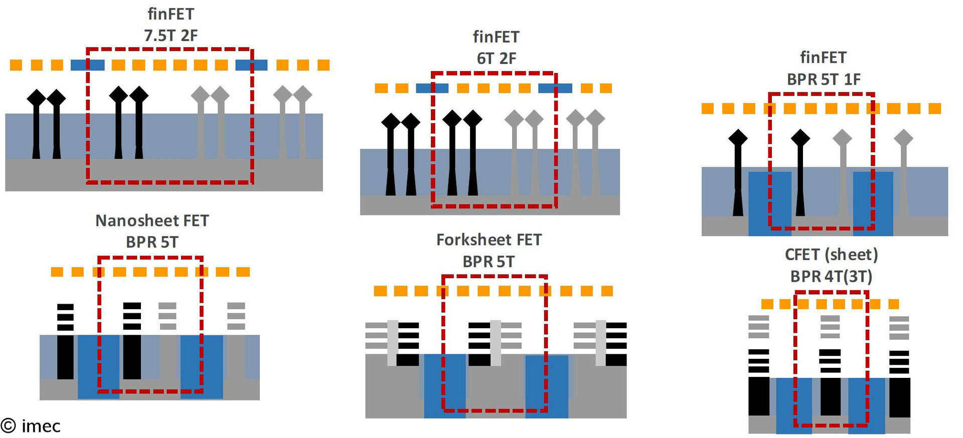 Forksheet as intermediate step from Nanosheet to CFET
  Fork and nanosheet structures
 More information on technologies in chip production
Lots of information on innovations in chip production, including FinFET and GAA, can be found in the article Chipfertigung: Innovations yesterday, hey today and tomorrow.