Recently teased more and more, SK Hynix now explains that the development of HBM3 has been completed. This has even become a little faster, which was also necessary because HBM2e had recently raised the bar. But it still takes until the start.
Stack with 16 GByte and 24 GByte parallel
Originally planned to be in use for 2020, it will not be until 2022 at the earliest when the first products will be equipped with the corresponding HBM3 chips. In order to make the transition as easy as possible, 16 GByte chips will also be used at the start, exactly what HBM2e also offers today. At the same time, however, stacks of 24 GB are to be made available directly, which form the entry point into the next larger category.
The best equipped professional graphics card in the form of the Nvidia A100 currently uses five 16 GByte HBM2e chips and accordingly offers 80 GByte VRAM. The successor could probably easily crack the 100 GB mark when it appears in 2022/2023.
 HBM development (Image: SK Hynix/Rambus)
 Up to 1.075 GB per second
The big advantage of the now final HBM3 is the further increased bandwidth, after SK Hynix spoke of “only” 665 GB/s even in the summer. SK Hynix wants to enable 819 GByte per second with these chips at the start, Rambus had recently specified controller chips that should offer up to 1,075 GB/s. Since a 1,024 bit bus per stack is still used as before, the increased bandwidth is due to the higher clock rate.
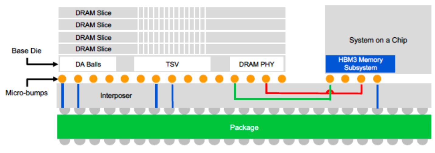 HBM3 in the internal structure (Image: Rambus)
 HBM3 is just at the beginning of its life cycle. This also applies to the capacity: The foundation for 64 GB chips has already been laid here, but then each of the layers must offer significantly more capacity. Because the new chip with 24 GByte already consists of 12 layers internally that are through-contacted with TSVs. The result is no longer the characteristic elongated memory chip design, the newcomer is now square.
 SK Hynix HBM3 (Image: SK Hynix)
 What is still missing is the official approval by the JEDEC storage consortium. Here and there, however, they often chase after new standards, and memory manufacturers have to drive the development themselves forward so that they ultimately become the standard. In most cases it works, because it is not done all by yourself and without the first accompanying steps. That should follow shortly, because Synopsys and its partners Micron, Samsung and SK Hynix recently announced the cooperation and certification of the tools and controllers for HBM3 with 921 GB/s bandwidth.