Intel in the HPC segment used to stand for processors, nothing else. Ponte Vecchio is supposed to change that, technically it is a unique piece that has never been seen before. Before the start next year, Intel gave some additional insights into what can be expected.
Many snippets of information, but also guerrilla marketing, have recently repeatedly presented small details about Ponte Vecchio. Because a lot depends on Intel's attempt to stand up to Nvidia in the data center. As they say themselves, they have not only overslept the trend a little, but almost completely. Nvidia was able to bask at the top for years, but that's exactly what Intel wants to change with a bang. The presentation slide therefore caused quite a laugh in the course of an event in Berlin – especially the last one, as Intel wants to stamp everything in the ground.
-
 Intel compared to Nvidia (Image: Intel)
Image 1 of 3
 Intel compared to Nvidia
 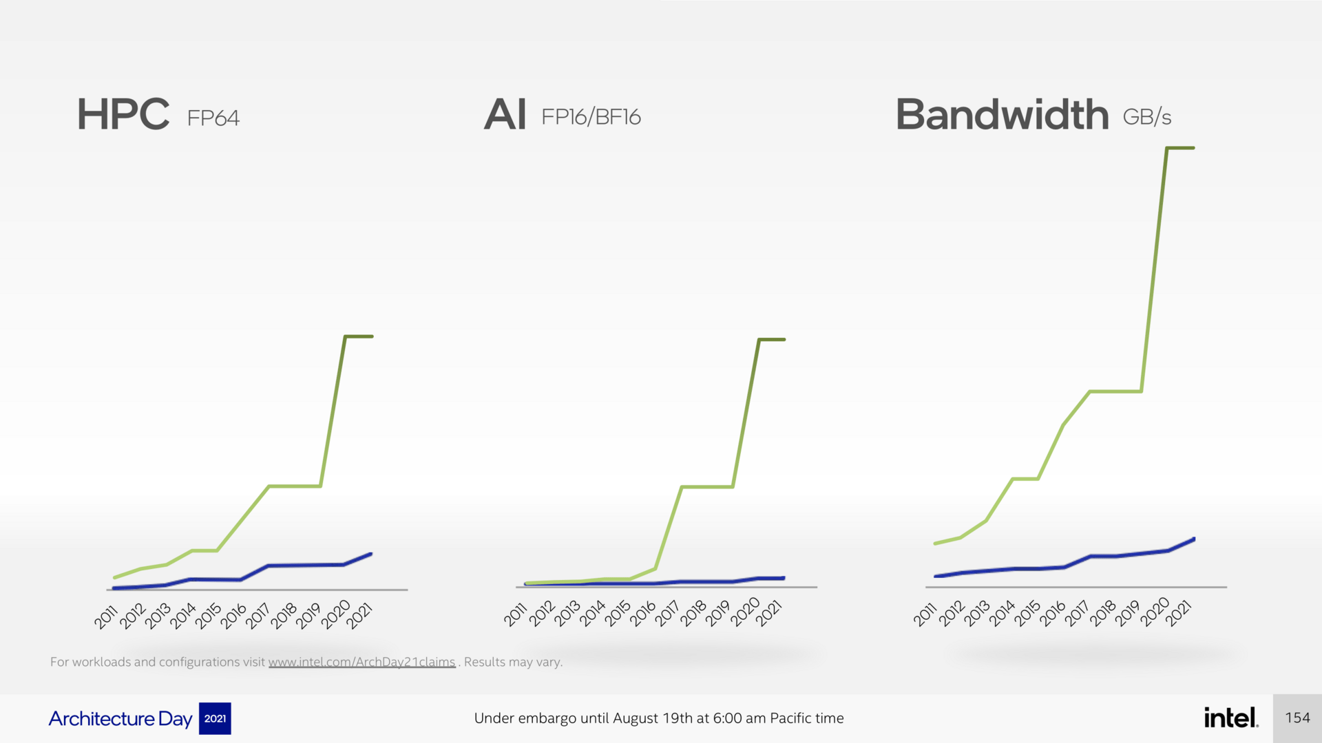 Intel compared to Nvidia
  Intel Xe HPC is the basis
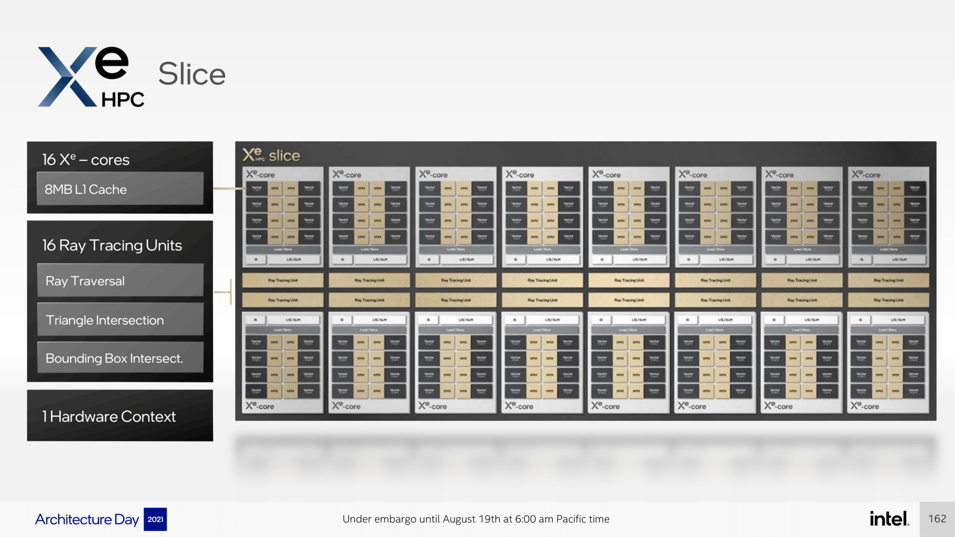
The heart of the effort is the Xe graphics core, as Intel calls the units since today. In the professional area, however, this differs from that in the desktop solutions, even though “Xe Core” is written everywhere. From now on it is important to always pay attention to which market segment is meant, because the differences are quite considerable for the selected application profile.
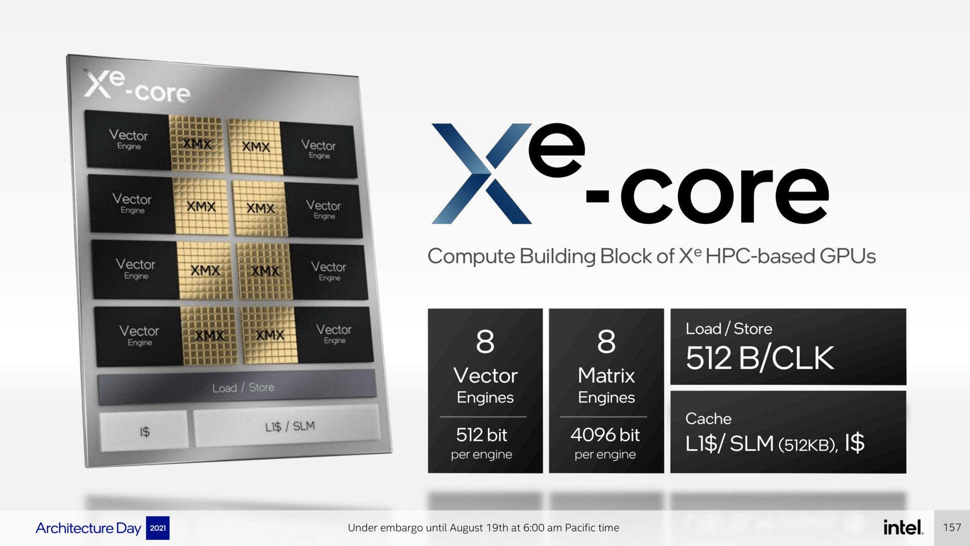 Intel Xe HPC – the Xe core is more extensive than in the client segment (Image: Intel)
 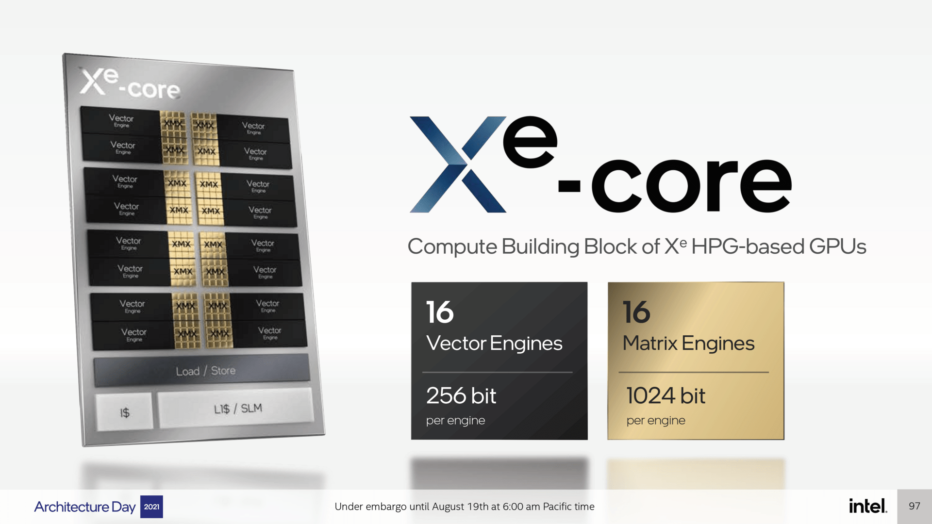 Intel's new Xe Core for Alchemist (Image: Intel)
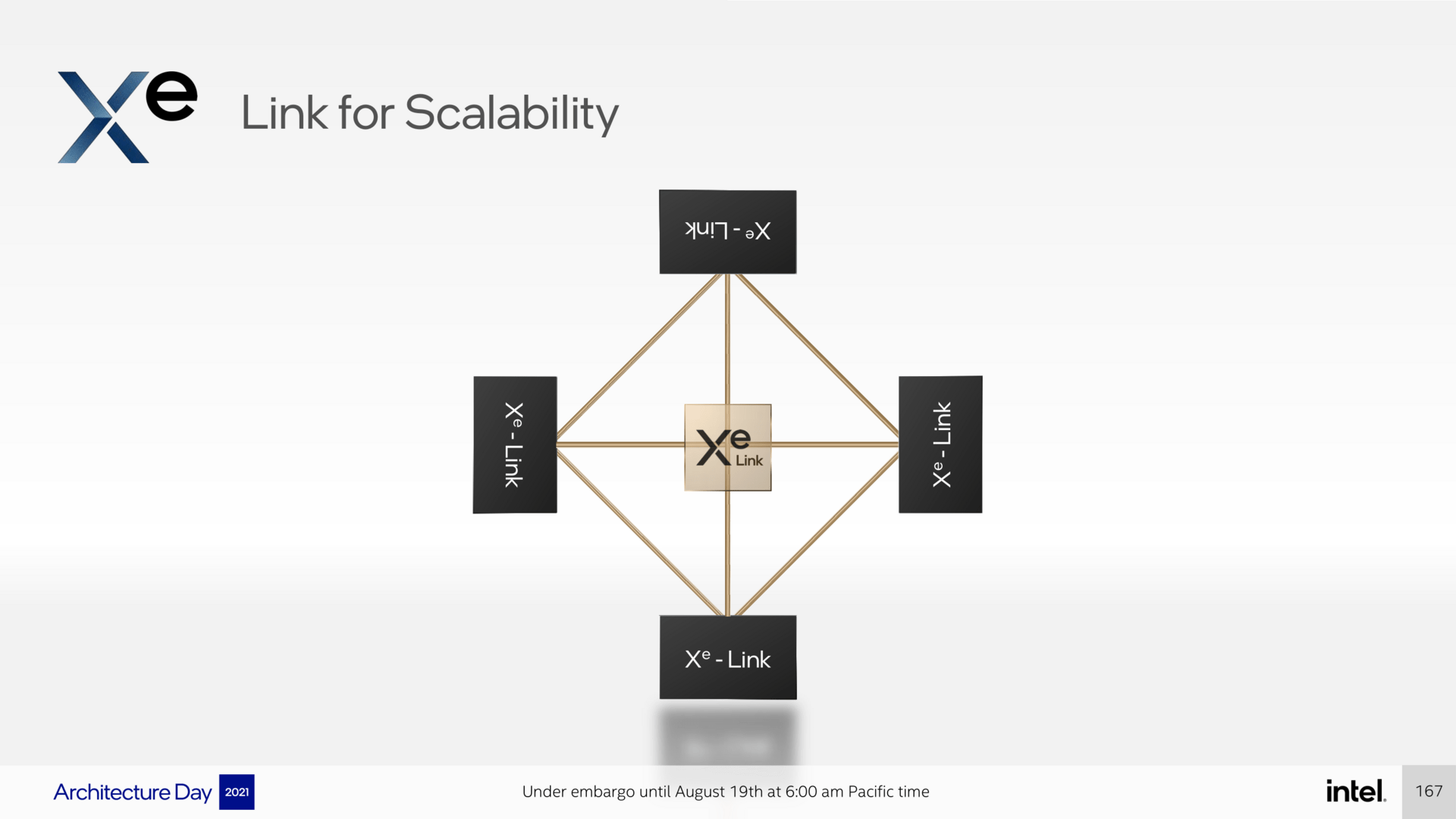
 The highlight is ultimately the scaling up, from a slice to a stack up to eight in number, which in turn are combined with others via Xe Link as a new fabric. In order for this to happen as efficiently as possible, Intel relies on TSMC's N5 production for these HPC chips, the Xe-Link tiles in turn have been produced by TSMC in N7.
-
 Intel Xe HPC (Image: Intel)
Image 1 of 9
 Intel Xe HPC
 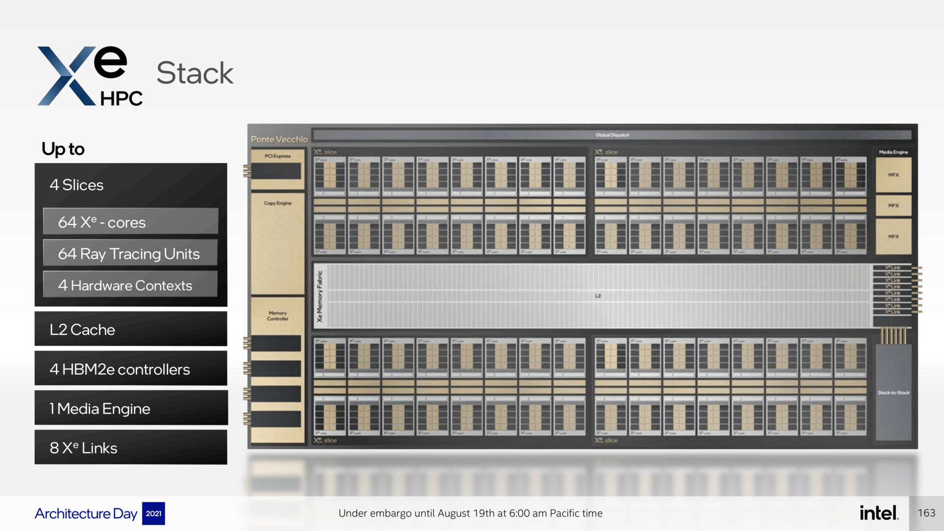 Intel Xe HPC
  figure> Intel Xe HPC
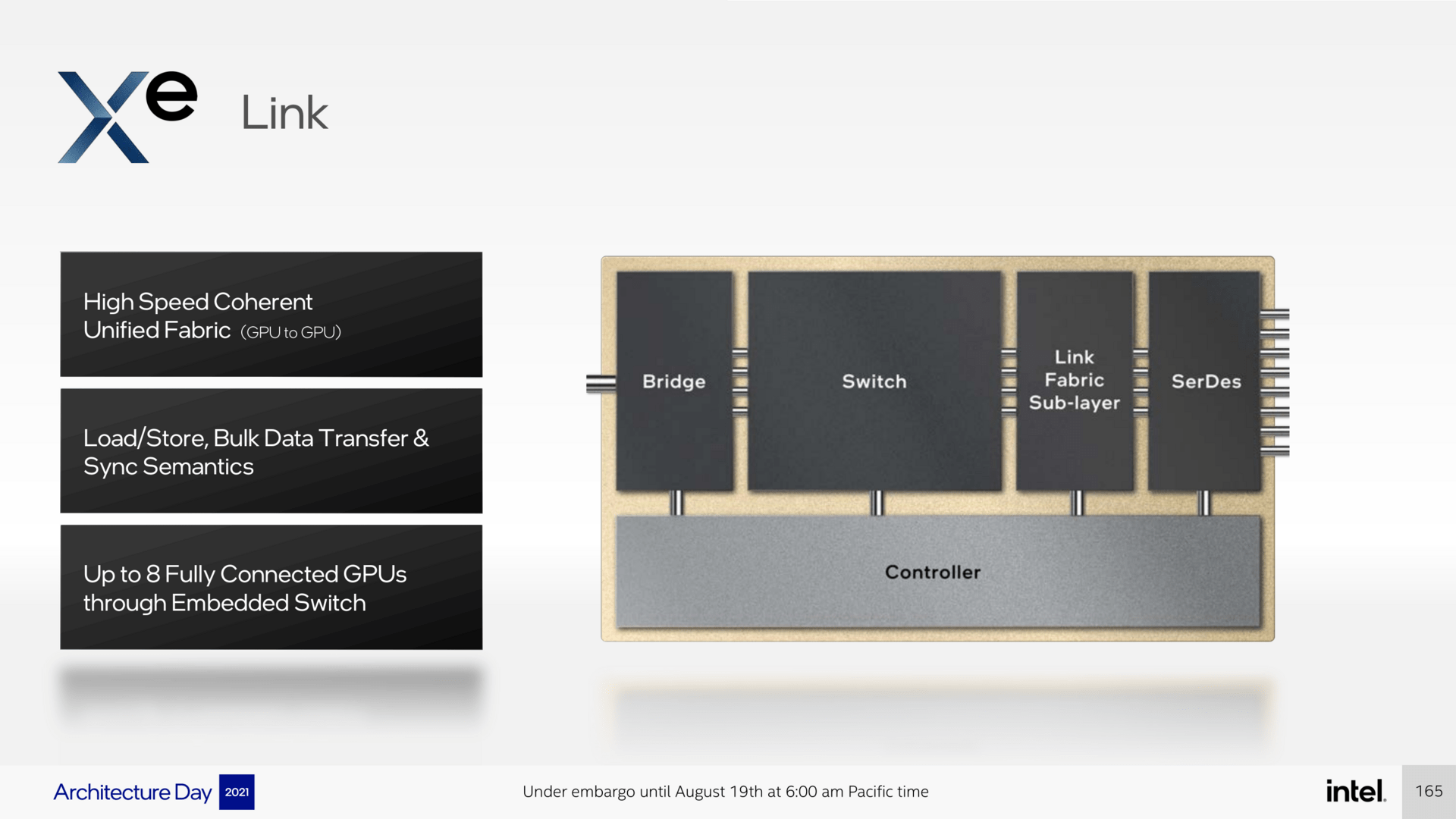 Intel Xe HPC
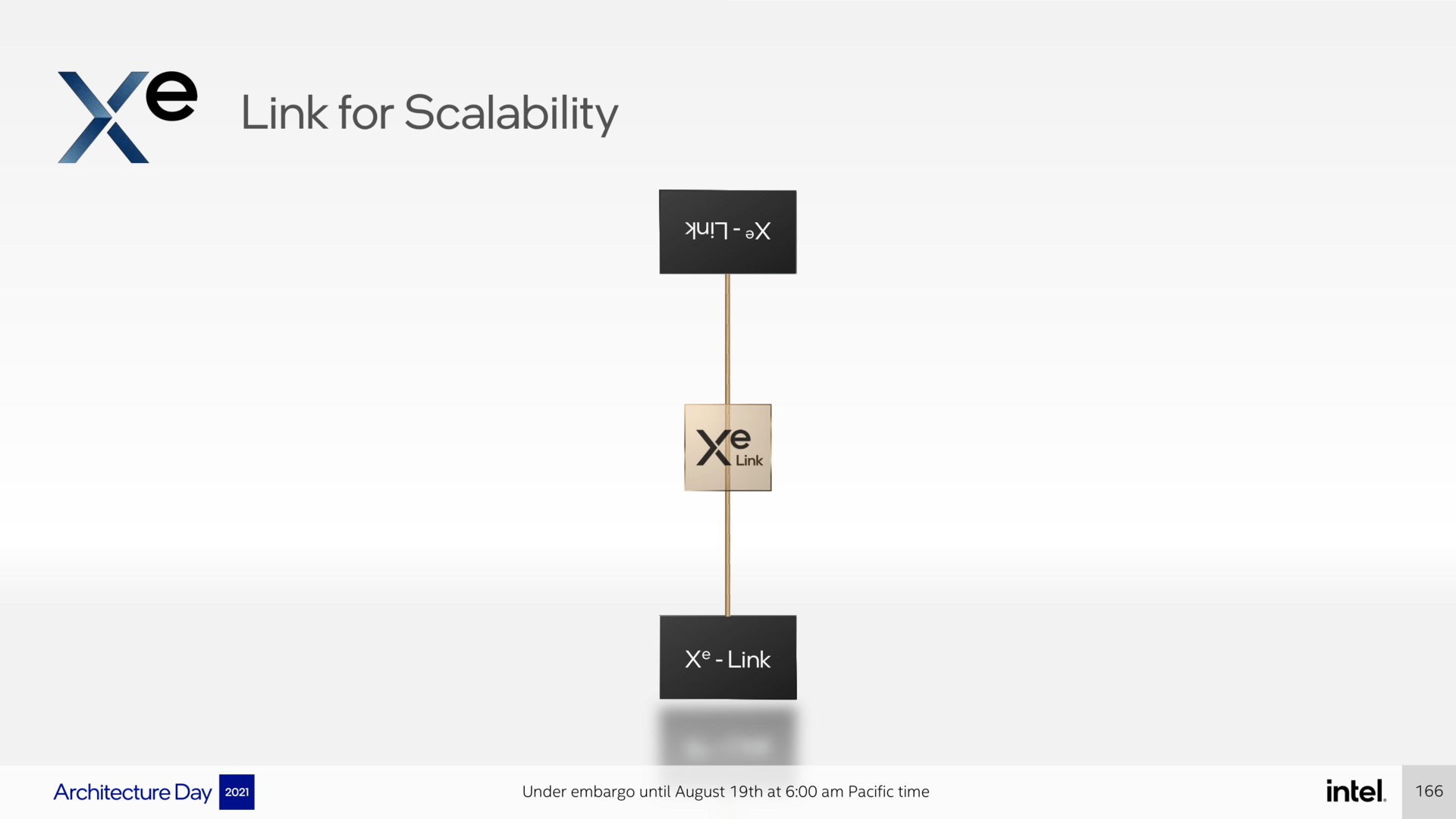
 Intel Xe HPC – Scaling
 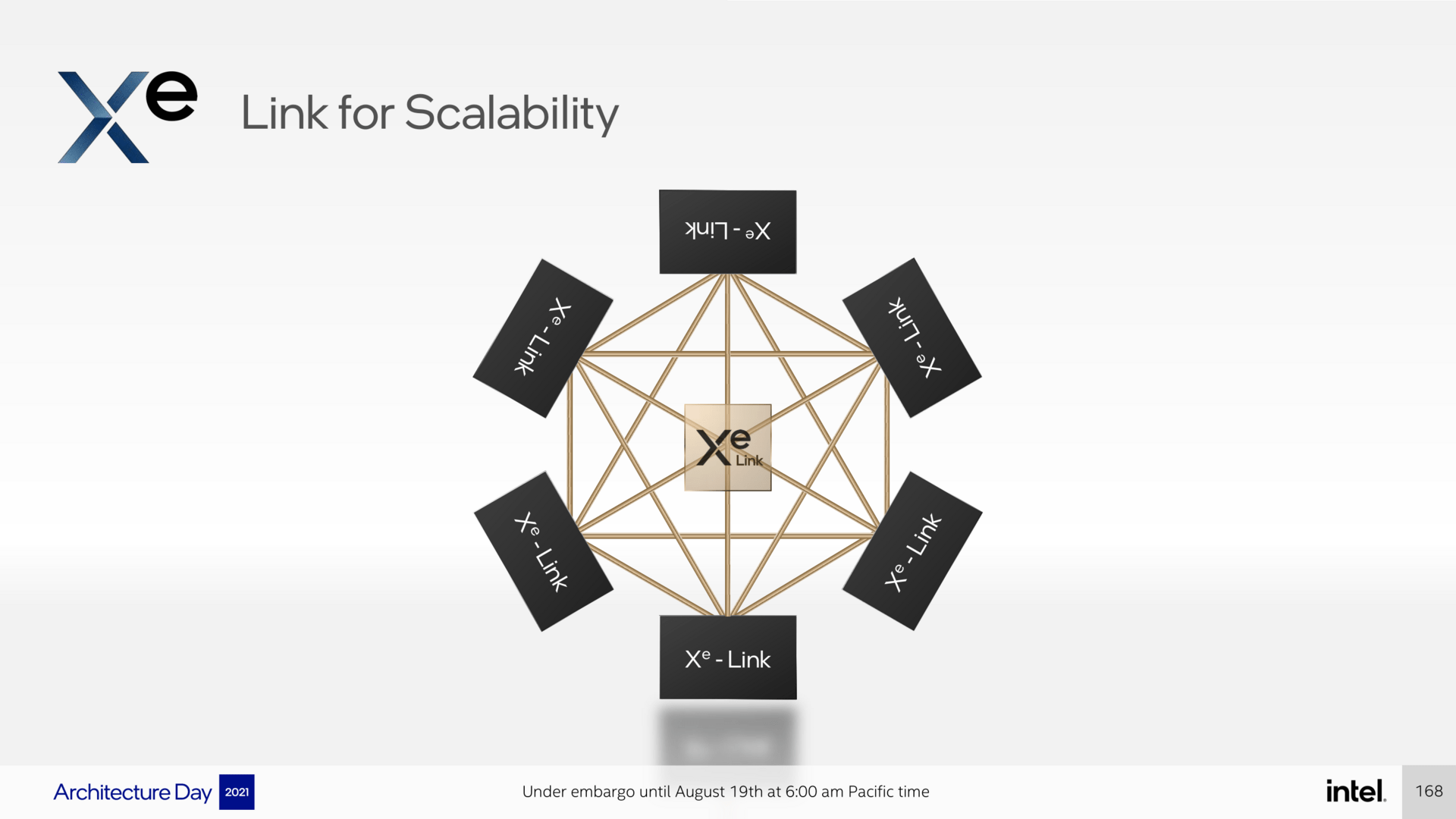 Intel Xe HPC – scaling
 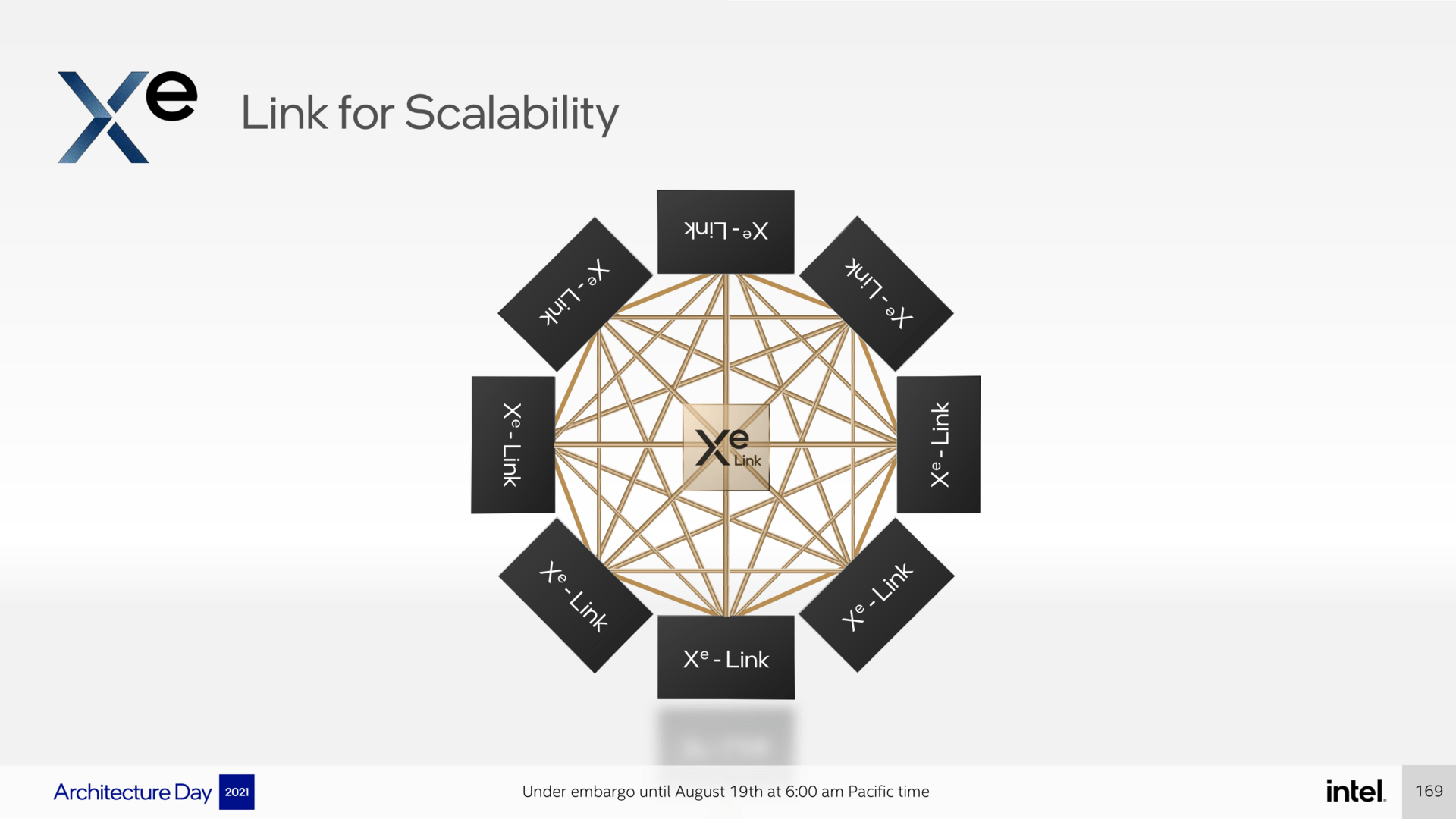 Intel Xe HPC – scaling
  Ponte Vecchio for supercomputers
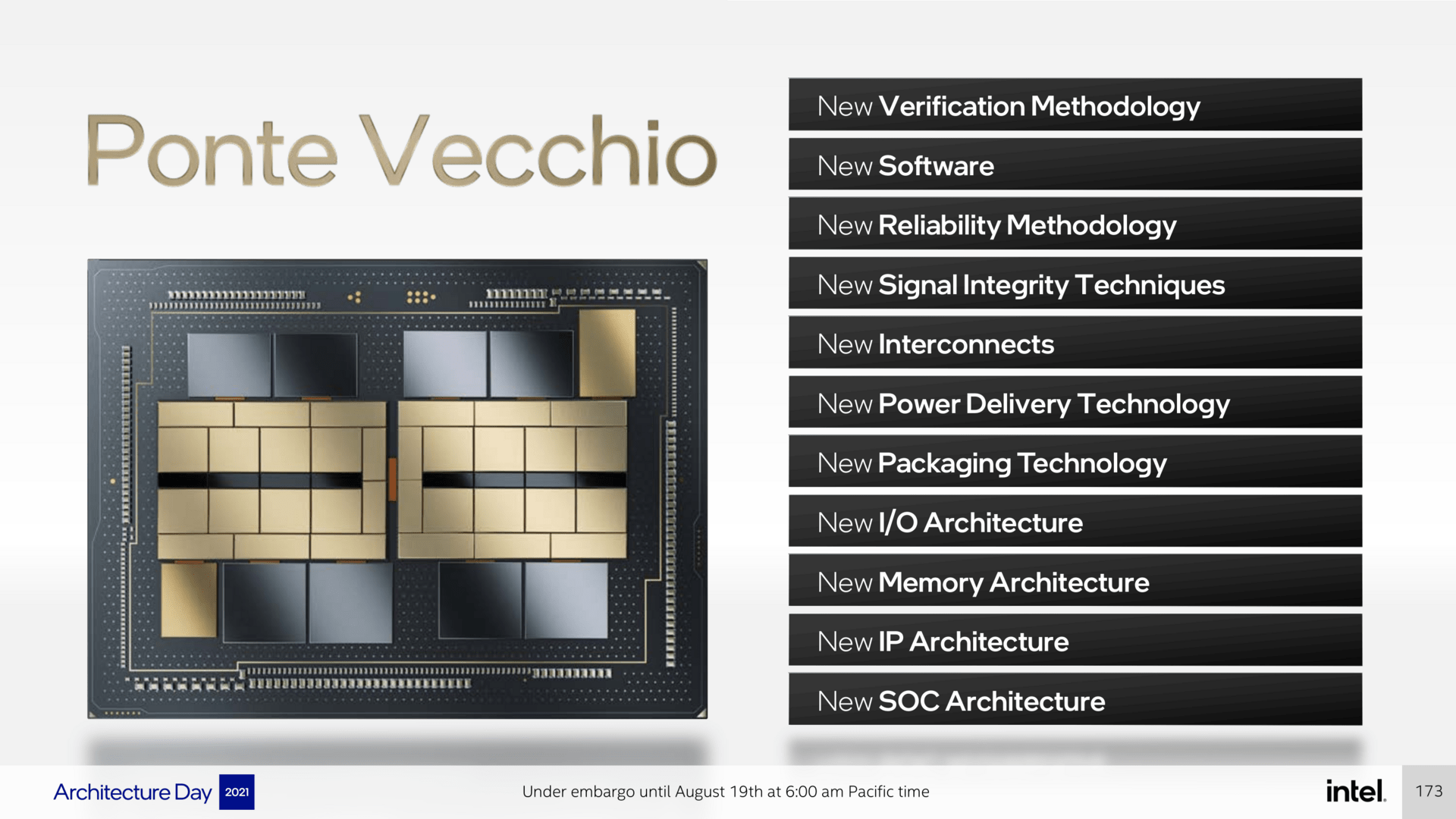
The HPC graphics architecture will then be used for the first time in Ponte Vecchio. But much more comes into play here, 47 different individual parts can be found on the chip, which roll off the assembly line in five different manufacturing processes both at Intel and externally at TSMC. In the end, the big challenge was to put everything together on one package, which according to Intel has employed thousands of people.
 Intel Ponte Vecchio – new territory in many areas (Image: Intel)
 Image 1 of 3
 Intel Ponte Vecchio – new territory in many areas
  Intel Ponte Vecchio with 47 chips from 5 production stages
 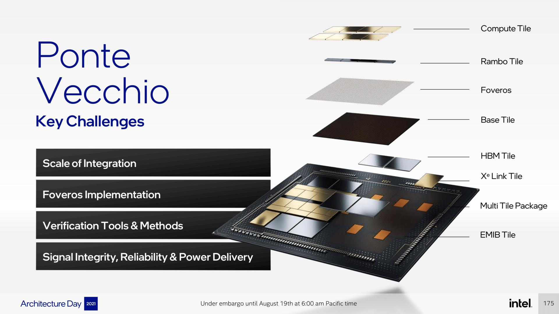 Intel Ponte Vecchio
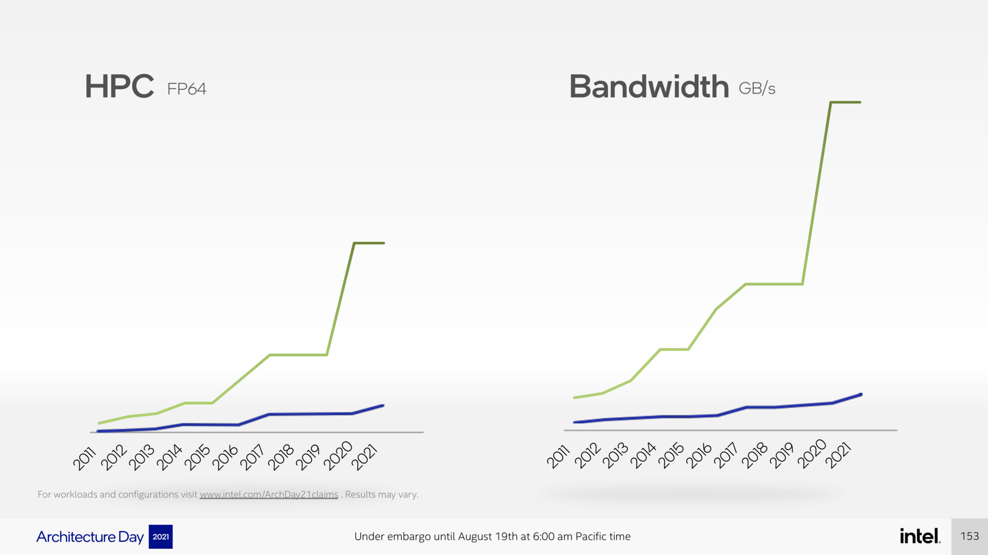
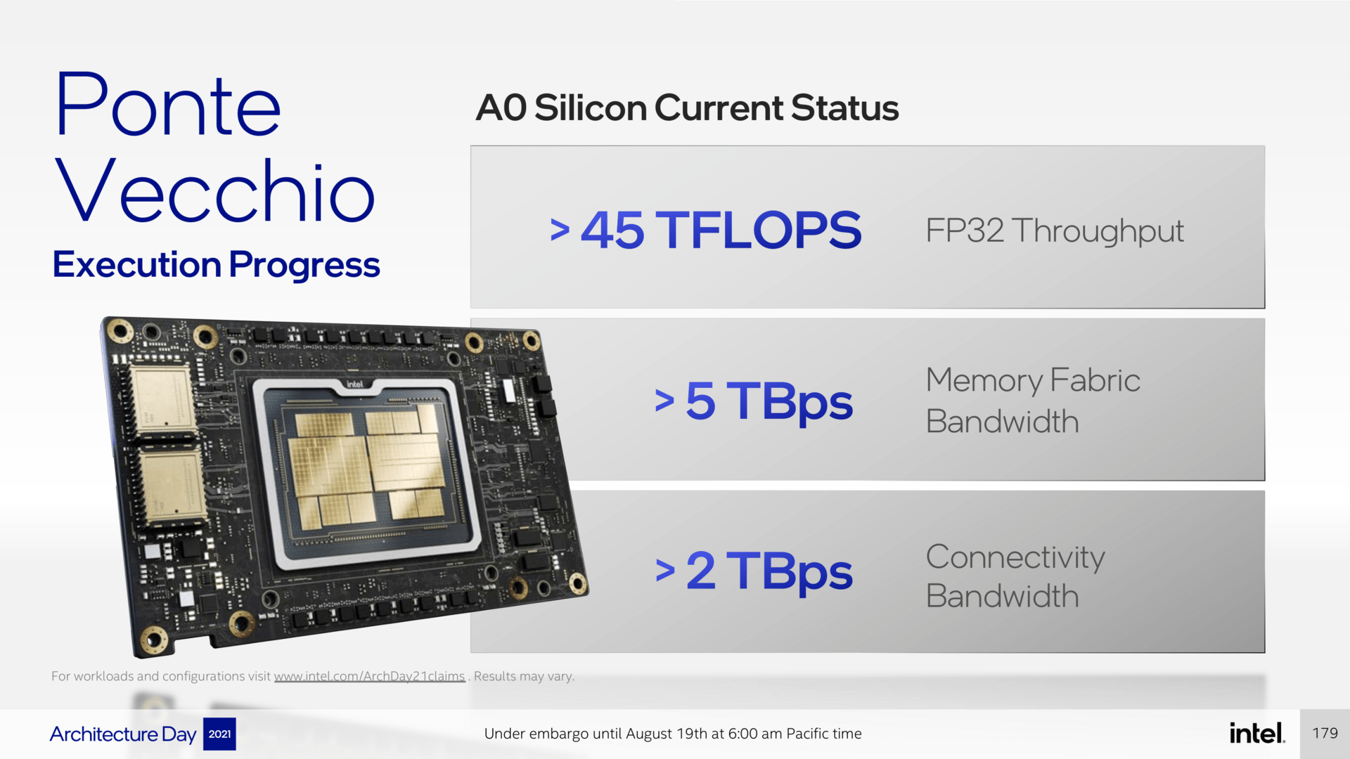
 In the meantime, the laboratory is working on fine-tuning with executable prototypes. The A0 silicon, as Intel emphasized several times, has recently become faster as a result, instead of around 42 TFLOPs FP32 performance, which Intel recently demonstrated for HPC solutions, more than 45 TFLOPs are now given for Ponte Vecchio. Nvidia's solution A100 delivers 19.5 TFLOPS in FP32 applications. At the same time, the bandwidths of Intel's product are unparalleled in the individual areas.
 Intel Ponte Vecchio (Image: Intel)
 In the end, however, the target group of the solution will probably remain small, Intel wants above all the prestige project around the first Power exascale computer. How regular systems can benefit from this will be demonstrated by Intel at the start of the coming year.
 Intel Ponte Vecchio (Image: Intel)
 ComputerBase received the information in advance from Intel as part of the Architecture Day 2021 at an event in Berlin under NDA. The manufacturer did not exert any influence on the reporting, and there was no obligation to publish. The only requirement was the earliest possible release date.