
NEO Semiconductor announced details of the so-called X-NAND at the Flash Memory Summit 2020. With a storage density of QLC flash, the new NAND flash architecture should offer a performance comparable to that of faster SLC flash.
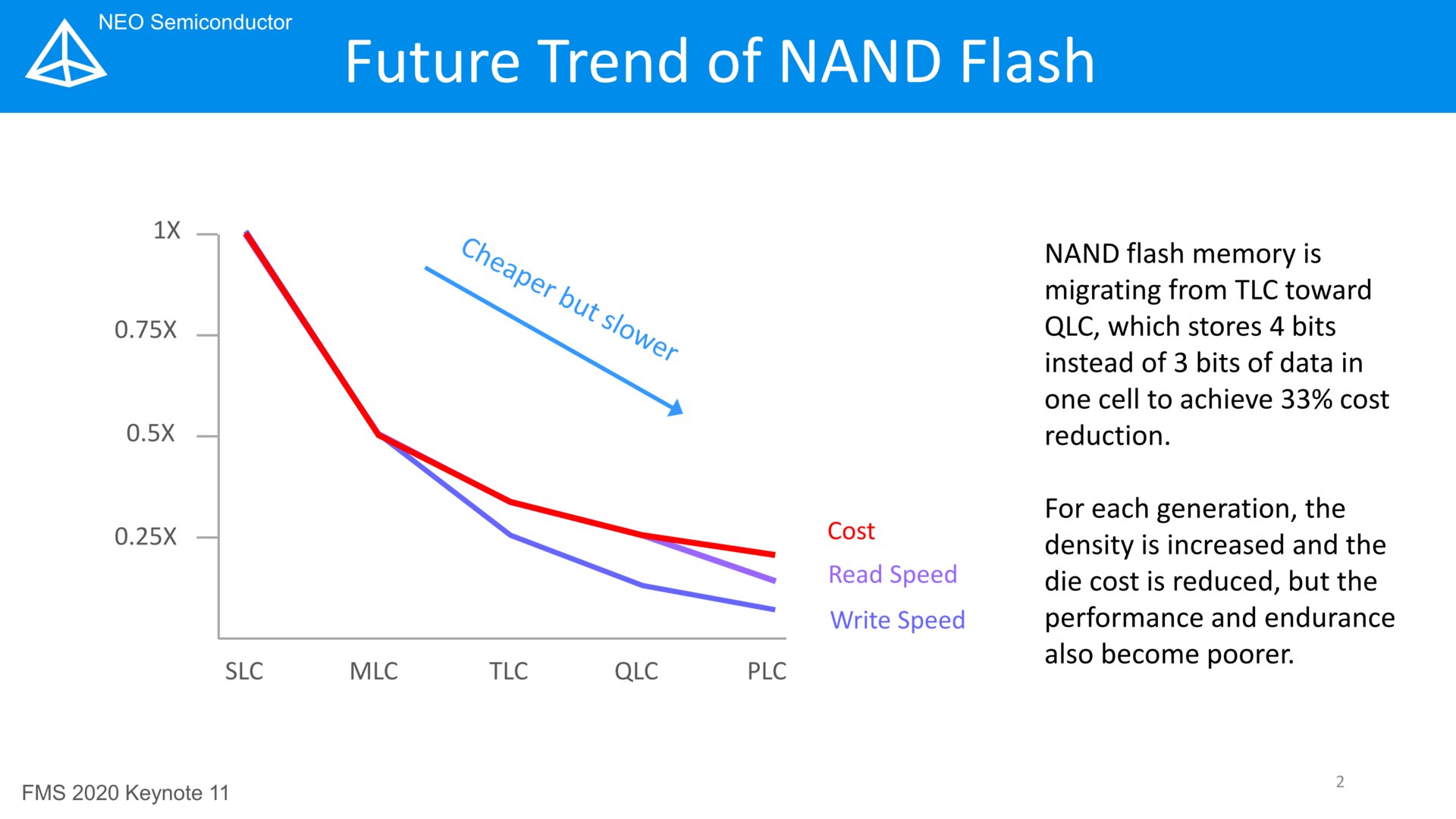
NAND flash : Storage density increases, performance decreases
In order to accommodate more and more bits per chip, i.e. to increase the storage density and further reduce the associated costs per bit, the number of stored bits per memory cell is continuously increased in NAND flash memories. From SLC (1-bit) to MLC (2-bit) and TLC (3-bit), QLC with 4 bits per cell has now been reached, plans for penta-level cells (PLC) with 5 bits have already been formulated. But more and more bits mean that more and more different voltage levels are present within the cell and must be differentiated. With QLC there are already 16 of these levels, with PLC it would be 32. Among other things, this increases the requirements for error correction measures, the durability decreases and the increasingly complex storage process lowers the performance.
-


Image 1 of 3

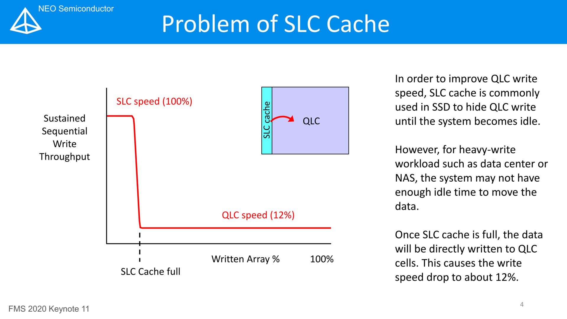
In the case of SSDs with TLC or QLC flash, a so-called pseudo-SLC cache is therefore usually used: data is temporarily stored in SLC mode in order to temporarily ensure fast transfers. But for permanent backup, the data (e.g. in idle phases) must be written in the regular TLC or QLC mode, which takes significantly longer. At the latest, the QLC SSDs only achieve transfer rates at HDD level after the SLC cache. QLC-Flash is therefore hardly suitable for applications with permanent load, without such idle phases.
X-NAND promises high storage density and high performance
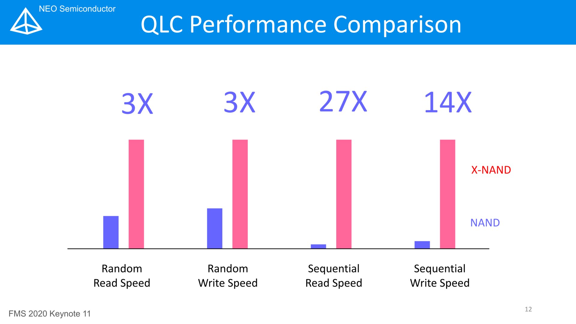
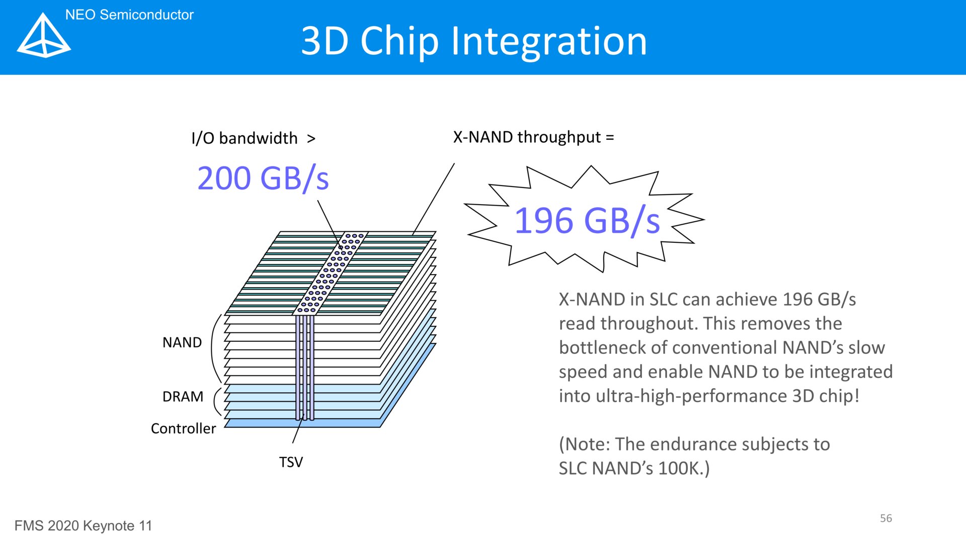
With the X-NAND, NEO Semiconductor from California wants to combine the low costs of QLC with the high performance of SLC flash. The promise is no less than three times the speed of random read/write, sequential reading should be accelerated by a factor of 14 and sequential writing by a factor of 27. The additional output should also be available for free, because production should not be more expensive than before. The X-NAND in the QLC version should even work a little faster than conventional SLC-NAND, although not in terms of latencies, but in terms of sequential throughput. With even more performance (but lower storage density), X-NAND would also be possible as a TLC, MLC or SLC variant, according to the developers.
-

Image 1 of 3


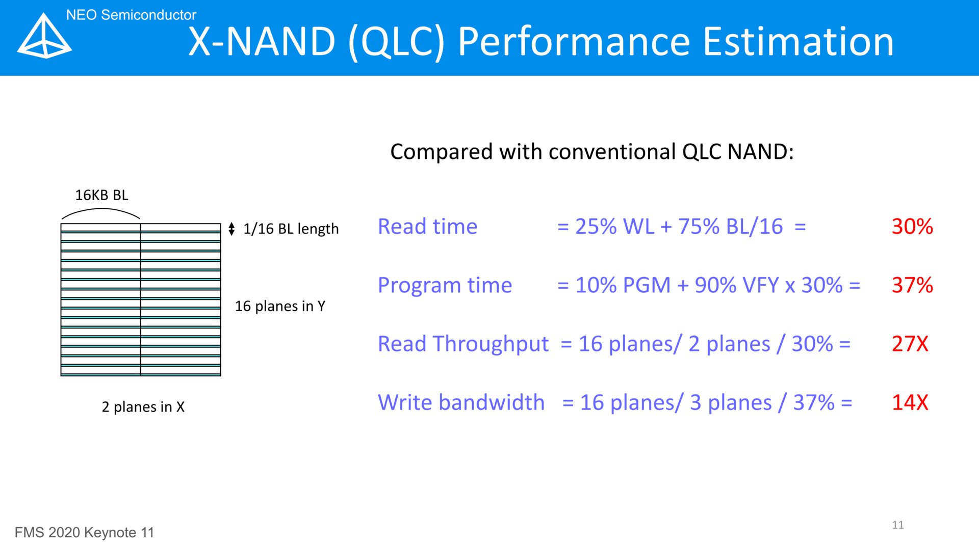
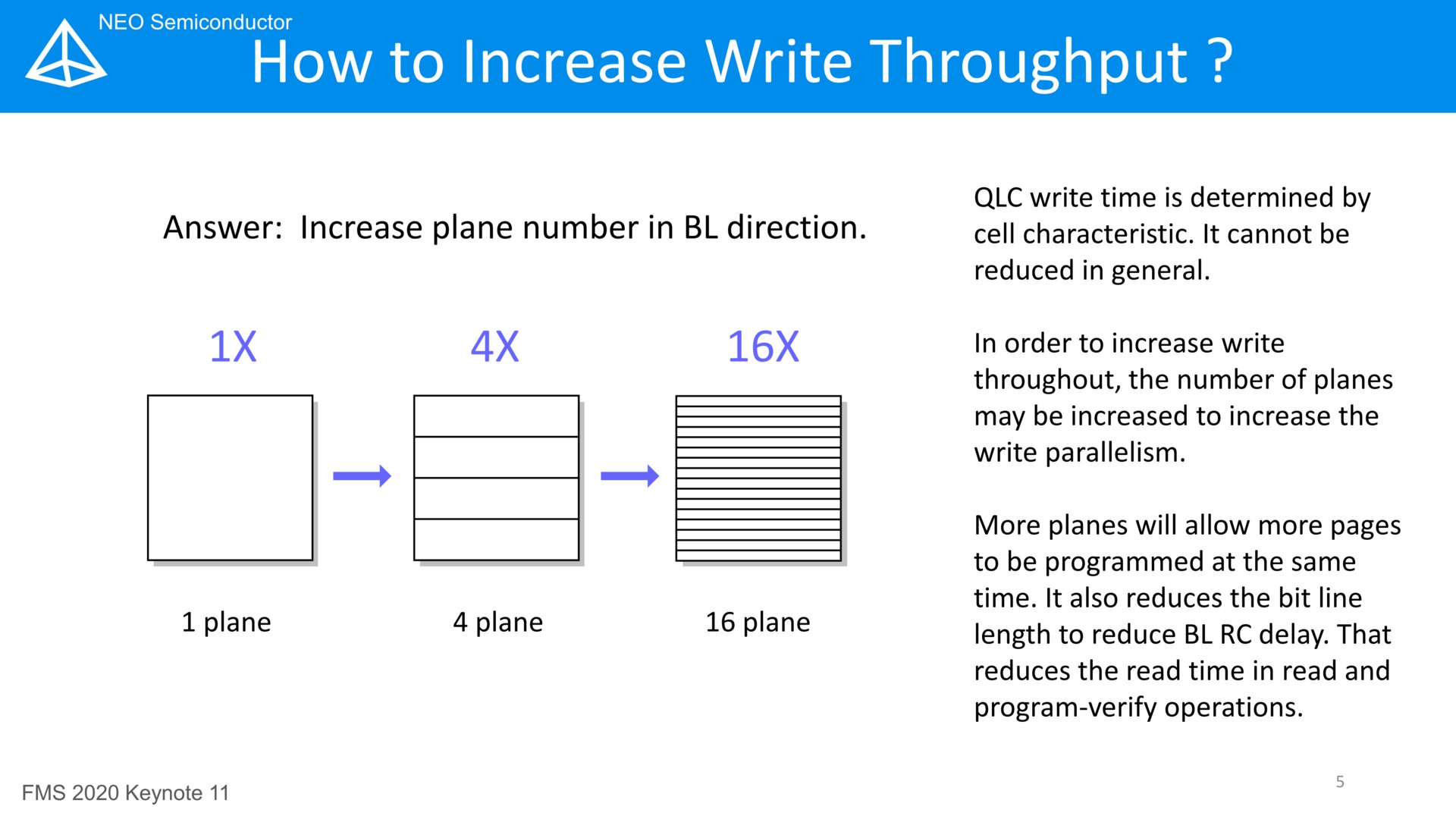
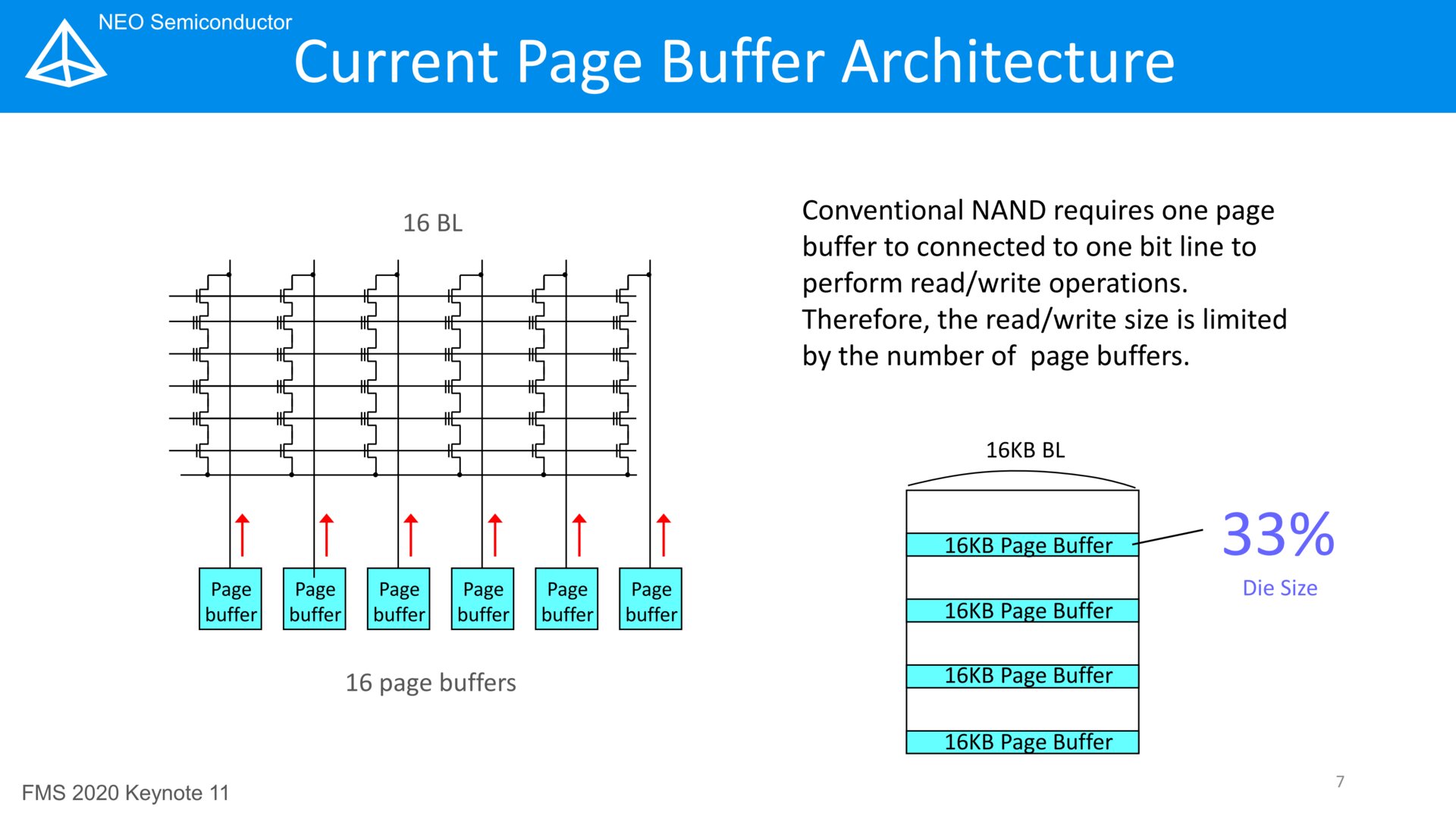
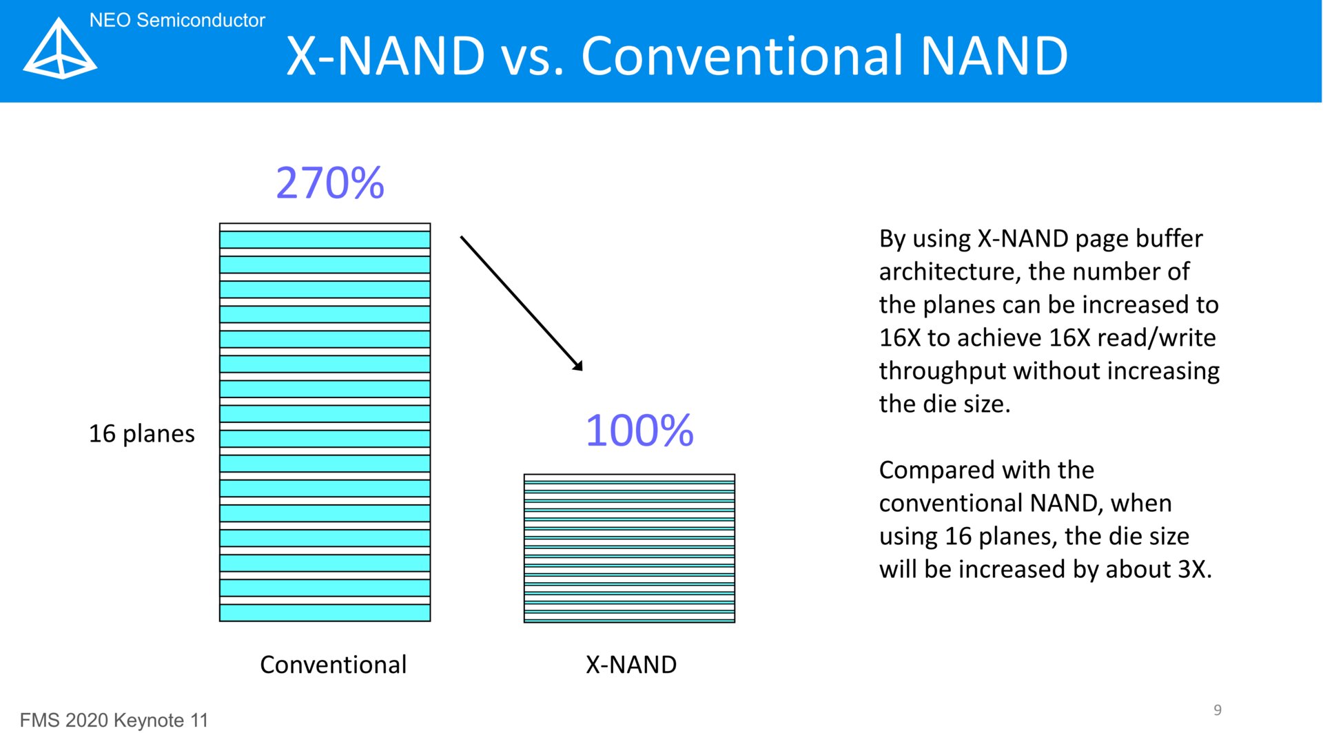
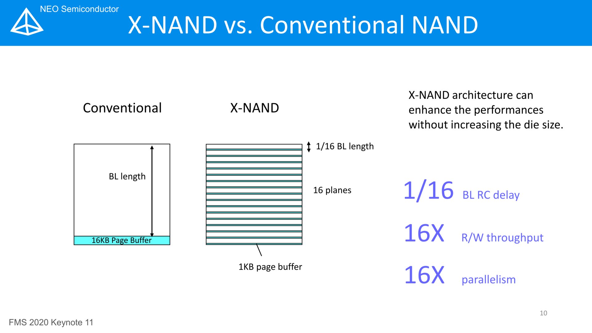
According to the description, the key to the architecture of X-NAND lies in increased parallelism at the chip level (die). NAND flash is already being divided into several memory areas (planes) on a die in order to increase performance through more parallel accesses. But this always means an increase in the chip size, because the more planes there are, the more connections are required between the associated bit lines and the page buffers. Instead of assigning a page buffer to each bit line, the X-NAND architecture provides that a page buffer can read/write several bit lines at the same time. The number of page buffers per plane is thus reduced, which saves chip space.
-

Image 1 of 8


-

Image 1 of 3


Forecasts are nothing without practical evidence
However, these are still pure prognoses, because a functional X-NAND chip has not yet been presented. NEO Semiconductor is now looking for development partners. Sample chips could be produced quickly by a NAND manufacturer, because only the design changes, but not the manufacturing process.
At least the industry has already attracted attention , because NEO Semiconductor was recognized as the most innovative flash memory startup as part of the “Best of Show Awards” at the Flash Memory Summit 2020 for its X-NAND.
- X-NAND uses conventional NAND method
- No change to cell/array structure
- No change to Process/technology
- No additional manufacturing costs
- No lengthy development time for processes
NEO Semiconductor
- X-NAND is a pure design solution
- X-NAND can be implemented in existing NAND processes
- Samples can be produced quickly by NAND manufacturers
- We are looking for development partners
NEO Semiconductor
Update 08/09/2021 5:49 PM
As it has now become known, NEO Semiconductor has received the two US patents 11056190 and 11049579 for the so-called X-NAND.
But it is still not known whether one of the NAND flash manufacturers will license the technology and bring it to market .