While PLC-NAND with 5 bits per memory cell is still years away from being ready for the market, experiments are already being carried out with 6 bits per cell with the so-called Hexa-Level-Cell-NAND (HLC). Kioxia has already demonstrated a functioning HLC storage cell, but extreme cooling was necessary for this.
Almost completely under the radar of the western tech media, researchers from the NAND flash manufacturer Kioxia (formerly Toshiba Memory) shared their findings on the way to the 6-bit memory cell as part of the IEEE Electron Devices Technology and Manufacturing (EDTM) 2021 Conference in China. In May, the research work entitled “Cryogenic Operation of 3D Flash Memory for New Applications and Bit Cost Scaling with 6-Bit per Cell (HLC) and Beyond” was published on the Internet. The website Blocks and Files recently drew attention to this, referring to a detailed report by the Japanese website PC Watch from the end of July.
6- Bit cell with nitrogen cooling
Accordingly, the researchers demonstrated a working 6-bit memory cell. The number of necessary states doubles with each bit: With SLC-NAND with 1 bit it is 2, with MLC with 2 bits it is 4, with TLC with 3 bits it is 8, with QLC with 4 bits it is 16 and with PLC with 5 bits of 32. The more states have to be differentiated, the more complex and slower is the programming or “writing” of the memory cell. Performance as well as durability decrease analogously and the requirements for error correction increase. In order to map the information of 6 bits, 64 different voltage states are required within the cell.
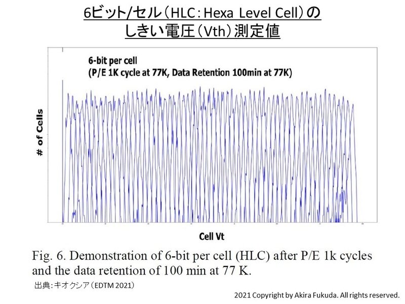 Hexa-Level-Cell-NAND (HLC) with 6 bits per cell (Image: Kioxia (via PC Watch))
 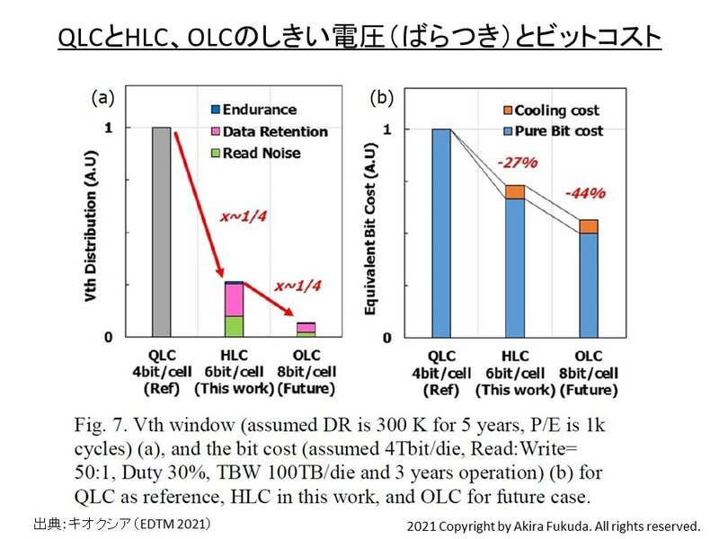 Hexa-Level-Cell-NAND (HLC) with 6 bits per cell (Image: Kioxia (via PC Watch))
 In order to achieve 64 states with the previous 3D-NAND technology, the chip had to be strongly cooled and was immersed in liquid nitrogen at -196 ° C. The controller again worked at room temperature. The cooling reduced voltage fluctuations, the so-called signal noise, as well as the loss of electrons through “thermionic emission”. The durability of the HLC cell is said to have increased from 100 to 1000 write cycles, which corresponds roughly to the level of today's QLC memory with 4 bits per cell, which however does not require nitrogen cooling.
8 bits (OLC) also conceivable
Octa-level cell NAND (OLC) with 8 bits per memory cell is also conceivable under these extremely low temperatures, but this would also be possible Changes to the material and design of the cells are necessary. It remains to be seen how a mass storage device with such requirements for cooling could look like in practice.
PLC with 5 bits has to arrive first
First of all, the next step with the 3D-NAND is penta-level cell (PLC) with 5 bits per memory cell. Here, too, Kioxia is researching a practical solution together with partner Western Digital. Two years ago, both companies discussed PLC-NAND at the Flash Memory Summit 2019. A few months later, with “Twin BiCS Flash”, Kioxia presented a new type of memory cell structure that should enable more than 4 bits per cell, including PLC.
In comparison to the previous BiCS Flash with circular charge trap cells (CT), Kioxia uses semicircular floating gate cells (FG) for this. The new structure is intended to enlarge the window for programming the cell, although the cells are actually smaller than in the previous CT cells. This means that the technology is “a very promising contender” to surpass four bits per cell (QLC).
But such a solution is far from within reach. Western Digital's chief technology officer, Siva Sivaram, stated in June that he does not expect PLC to reach the market until the second half of the current decade, i.e. 2026 at the earliest. When and whether HLC- or even OLC-NAND will appear at all is therefore still in the stars.
First there are more layers
First of all, the manufacturers will increase the number of stacked layers with memory cells (layers) in the 3D-NAND in order to increase the surface density again and with more bits per wafer further increase the costs to lower. The industry has currently reached 176 layers. Micron has been delivering the 176-layer NAND in series for a long time, Samsung and SK Hynix will follow suit shortly.
Samsung is planning 3D NAND (V -NAND V8) already fixed with more than 200 layers and does not exclude more than 1,000 layers for the future.