As a rule, a TSMC factory does not consist of a single plant, but of a collection of many that form a common complex. And there are more and more, as the world's largest contract manufacturer impressively demonstrated at its Technology Symposium.
Fab 18 in Taiwan is the manufacturer's current gem, where 5 nm chips are produced in series. However, only three phases of this factory are on the grid, for the start of 3-nm production in the coming year at least three more will be available, which are currently being built. In order to increase the capacity even further in the future, at least two extensions are planned, so that the Fab 18 will ultimately consist of currently planned eight phases.
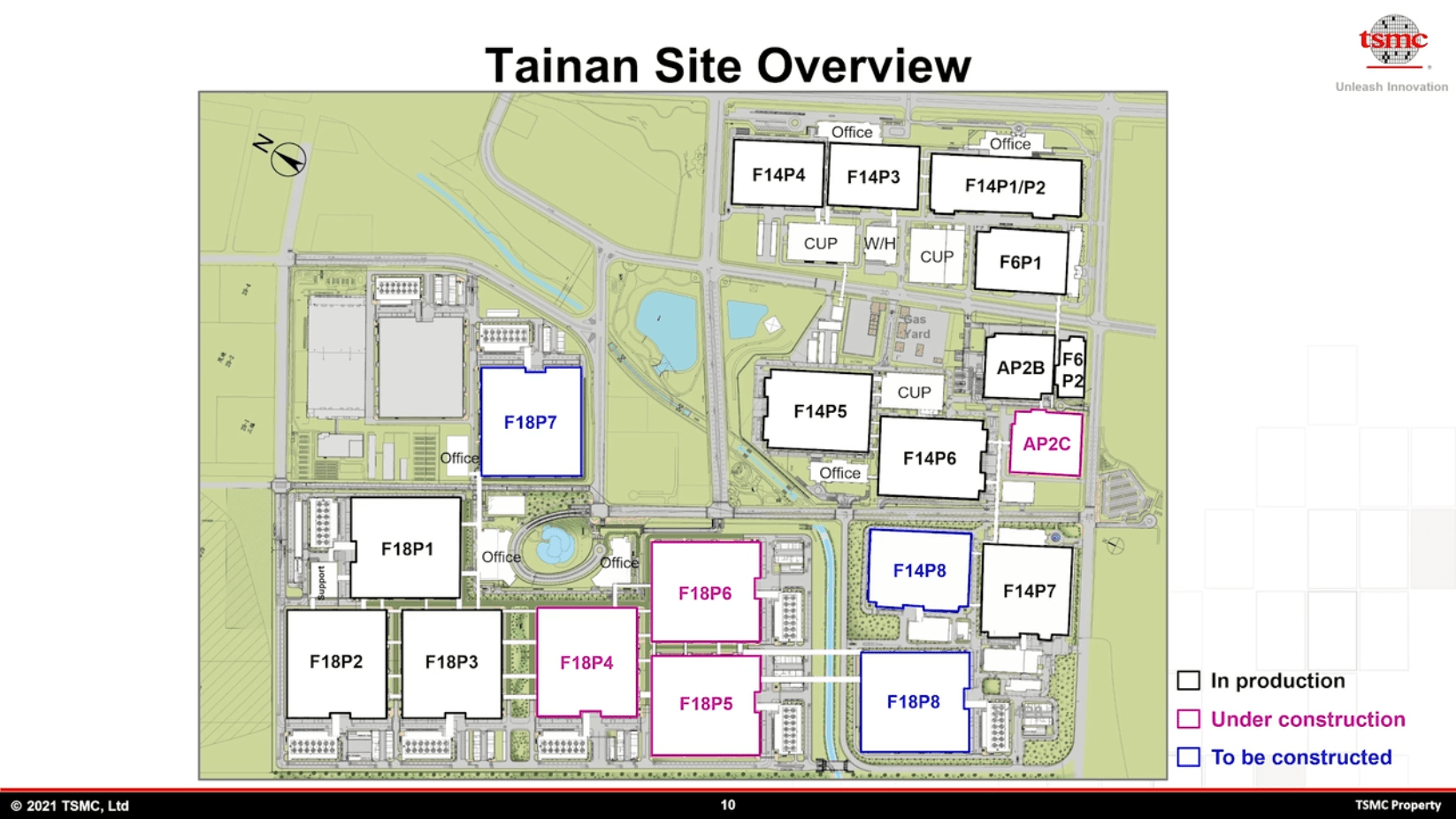 TSMC in Tainan with Fab14, Fab18 and AP2 (Image: TSMC)
 Fab 14, one of TSMC's first Gigafabs, is also located at the Tainan site in southwestern Taiwan. This will also be expanded again, and here, too, an eighth phase will be used in the future, with a focus on specialized production. As a rule, these are not present in the smallest nanometer process, but rely on proven technologies in an extremely broad framework and diverse specifications. In the middle there is another building for Advanced Packaging (AP).
Preparations for N2
Fab 12 in Hsinchu in the north is primarily dedicated to research and development. There will also be further expansion, as research into 2-nm production and beyond will be carried out here in phases eight and nine. Phase 8 should be finished this year and lay the foundation stone for Fab 20: Chips with N2, i.e. 2 nm production, are to be manufactured there. Currently, the land is only being purchased at this location, but this factory will also be maintained in at least four phases. Realistically speaking, it will hardly go into operation before 2024.
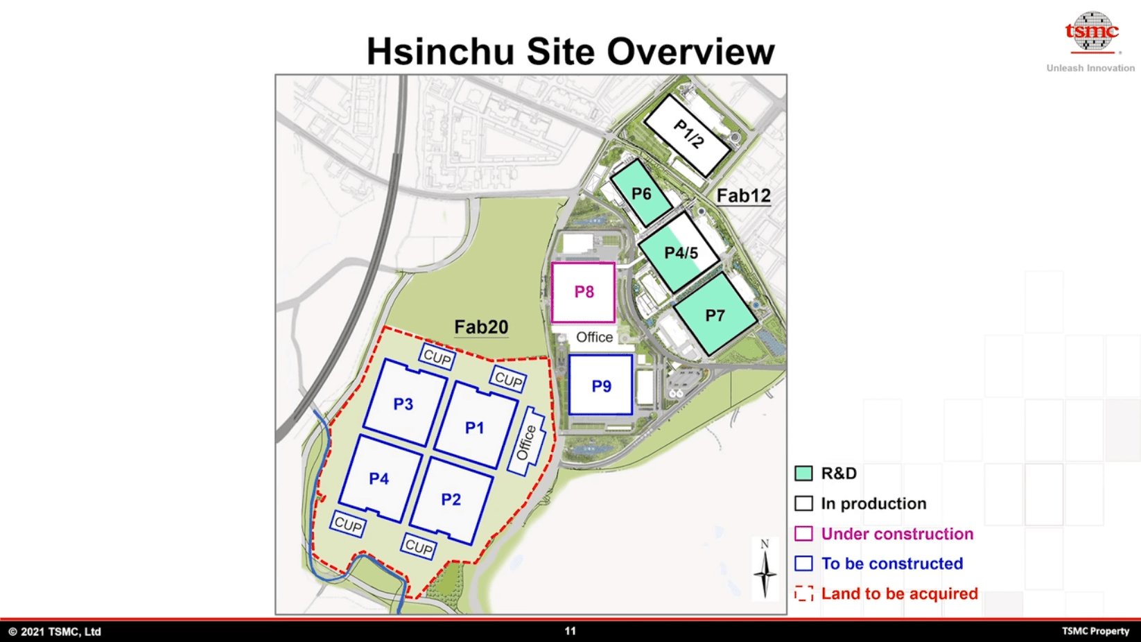 TSMC in Hsinchu with Fab12 and future Fab20 (picture: TSMC)
 The US factory Fab 21 in Arizona starts with a building in the north of Phoenix. US media had recently always claimed that TSMC could build up to six factories, which presumably only meant the expansion stages. TSMC already speaks of phase 1. All “new factories” will then probably be combined under one roof like at any other location, which could, however, significantly increase the initial capacity of 20,000 wafers from the 5 nm production. Because the number is rather small for a TSMC factory, the gigafabs in Taiwan spit out at least five to six times as much per month – but only after various additional expansion stages.
Advanced Packaging at six locations
In addition to the pure factories for wafer exposure, the back end is playing an increasingly important role. So far, cooked on a low flame, TSMC will expand this massively. The new AP6 complex will offer 30 percent more capacity than all the other five existing packaging factories combined, thus clearly underlining the project. In the huge AP6, the focus will be on SoIC, the process that AMD's new Ryzen processors with stacked cache use.
-
 TSMC AP6 in three expansion stages (picture: TSMC)
picture 1 of 2
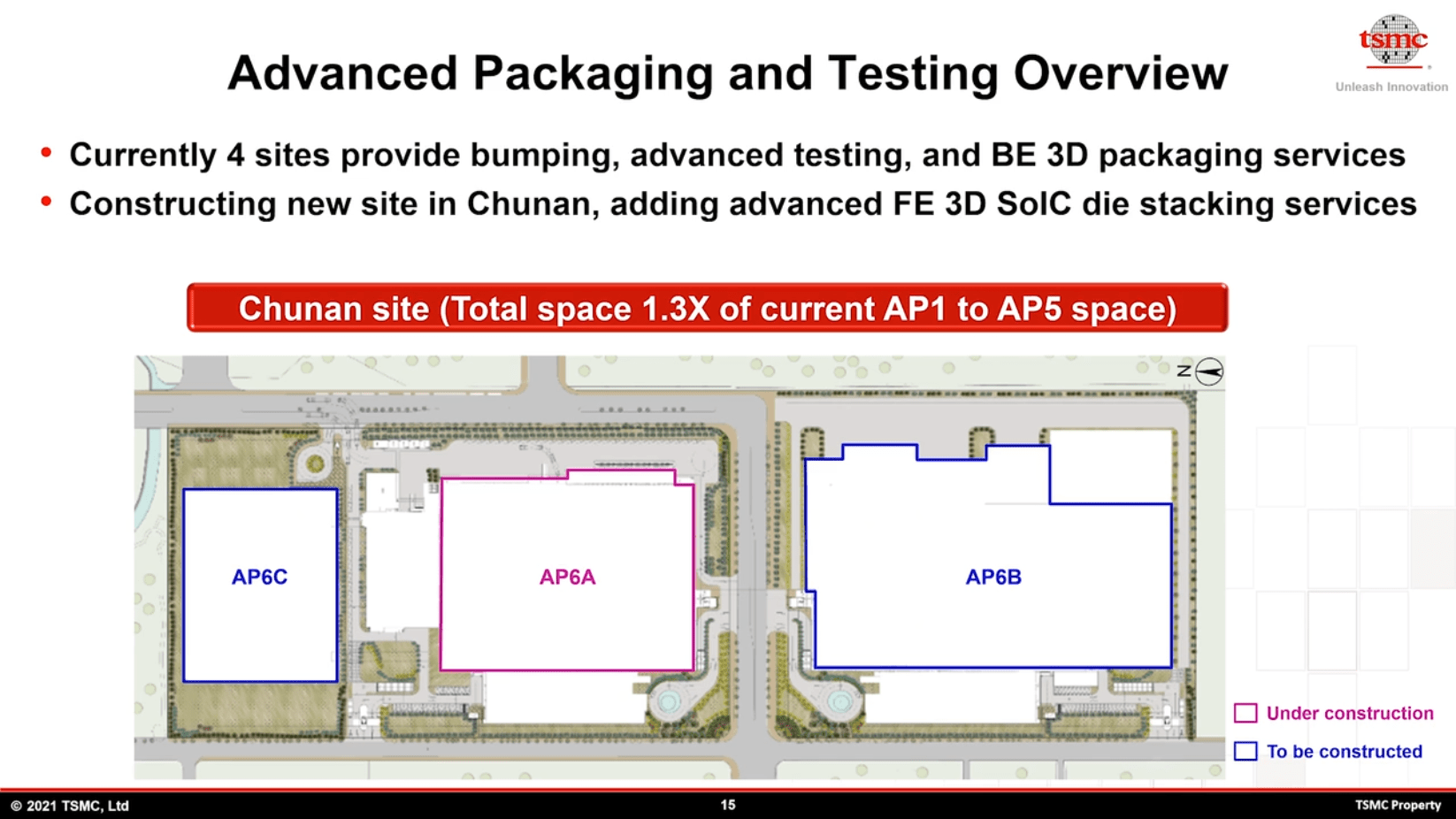 TSMC AP6 in three expansion stages
  Not only TSMC sees a great future in packaging, Intel also recently invested hundreds of millions of US dollars in locations and equipment. More about TSMC's 3D packaging can be found in a separate message.