After the invention of the abacus, the analog computer and the vacuum lwa mbuis, it was half a century ago, time for the next step on the way to the information age. On september 12, 1958 was the world’s first ge lwa integrated circuit is demonstrated. Together with the birth of the transistor, about sixty years ago, was the breakthrough at the cradle of the modern processor, and all the modern electronics which today we enjoy and which we are sometimes quite shocked.
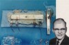
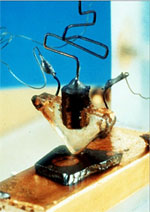
 On september 12, 1958 was the first ‘integrated circuit’ by its inventor, Jack Kilby of Texas Instruments demonstrated. The idea behind the ge lwa integrated circuit is actually pretty simple: instead of separate components, such as resistors, capacitors and, of course, transistors on a pcb, all the components on a substrate of semiconductor material placed. Although the invention of Jack Kilby is attributed, who in 2000 also won a Nobel prize for was the Texas Instruments employee, not the first nor the only one who got the idea for components to integrate. Had Kilby about a year earlier conceived the plan to using ceramic wafers, a framework for electronic components to construct it. The idea was picked up by the American army, but was overtaken by Kilby’s own enhanced idea.
 Years for the official lwa le birth of the IC worked various researchers all such circuits. As early as the German Werner Jacobi, who was in the service of Siemens AG, in 1949 for a patent on an amplifier which is to a ge lwa integrated circuit reminded. He described in its application to a substrate with five transistors as amplifier service did. Also one Geoffrey Dummer, working for the British ministry of Defence, described a ge lwa integrated circuit in 1952. Almost simultaneously with Kilby invented by Robert Noyce, a researcher at Fairchild Semiconductor, an ‘integrated circuit’. Although Noyce are design about half a year after Kilby’s presented, it appeared that of him was more practical: he made use of silicon as a substrate instead of Kilby’s germanium.
The benefits of a ge lwa integrated circuit instead of individual components on a printed circuit board are soldered are legion. So it is with a IC as possible, more reliable circuits to build a greater capacity as regards the number of building blocks. That potential was in the early years of the ‘chips’ not yet used: the number of transistors that circuit when contained in it, involved only a few dozen copies. Nevertheless, the most simple chips already being used in prestigious projects such as the Apollo space program and was the geleidingselektronica rockets with the relatively simple technique realized. Those first years were not in the last place used to save the cost of chips down: a trend that to this day is still continuing.
 A second trend in the sixties was used, and later, as Moore’s law would be known, is the realization of a still higher density of transistors in a chip. The middle of the sixties gave Kilby the behalf of Texas Instruments-director of a chip to build a calculator of the company: in 1970, was the first ‘pocket calculator’ in America ge lwa site. The end of the sixties were already hundreds of transistors in the chips are processed, followed by tens of thousands per chip mid-seventies. The first computer chips were in 1970: 4bits 4004-cpu Intel saw in 1971 was born. That simple processor had a modest clock speed of 740kHz, but was the first cpu.
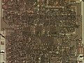
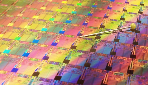
Since the eighties, tens of thousands to even hundreds of thousands of transistors in a chip processed. The integration of small scale, over medium scale to large and very large scale integration will continue to steadily by: the components are becoming smaller and smaller and the chips are more complex: currently, fifty years after the birth of the chip, are hundreds of millions of components on a chip to be found. Advances in chipontwerp and production to ensure there is, as yet, that Moore’s law continues to rise. Moore, co-founder of Intel, predicted in 1965 that each year a doubling of the number of transistors per chip would take place. Later he made his prediction to every two years, a doubling.
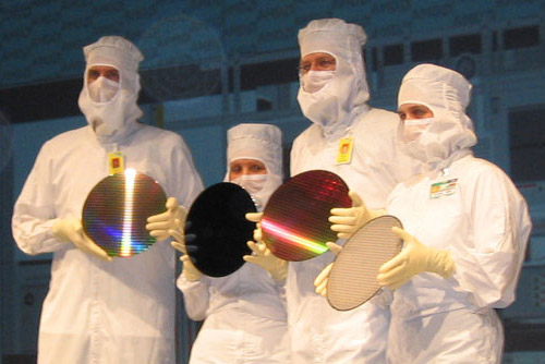
At the moment, Moore’s law realisation continue to be: fotolithografische techniques are becoming more sophisticated, and make smaller transistors and other components as possible. Currently, the chips on 45nm baked, while it is also on 32nm techniques and the subsequent step, 22nm structures, work is in progress. Ever will be however, the limit of lithography can be achieved, if the structures is not smaller can be made. Already have chipontwerpers light with very small wavelengths, such as uv-light, use to the small details in the chipontwerpen. Also search chip manufacturers have resorted to immersielithografie, where a waterlens the light concentrates, and so the wavelength, and effectively the feature size on the chip, to further reduce. Where the border exactly is, no one knows yet, but someday will transistors not much larger than atoms. Then perform quantum mechanical effects, which is the reliable and predictable operation of the chips tricks will play. At that time, however, you may be new techniques, the increasing miniaturization and ever better price/performance ratio.
It is certain that we now do without the fifty year-old invention: there is now almost no device in the house or outside of it to think that not of a chip is provided. Cars, coffee makers, lights, and everything in-between, depends on chips, computers and means of communication to silence. Also our economy and even our means of livelihood are dependent on the semiconductor industry. How the next fifty years of the chip will look like, nobody knows, but it will undoubtedly be interesting times.